


Important Links
Product Page
Assembly Instructions
Bill of Materials
Schematic
Capacitor and Resistor Lookup Guide
Welcome to the assembly instructions for the Clock Capture Module. This device captures the frequency from the right channel from any audio source and converts it into a clock pulse.
This is one of our older designs with a more basic silkscreen on the PCB, meaning that to assemble this circuit correctly you will want to pay close attention to the instructions and follow them closely to build a functioning circuit.
BOM Layout
If you’ve received your parts and ready to build, the first thing you should do is to check to make sure you have all the parts. Check your kit against the Clock Capture Module BOM. If you’re missing anything we’ll send it to you free of charge.
Attention: Changes may occur after the Assembly Instructions are created and the photos may not reflect those changes. Always use the BOM to verify the placement of components.
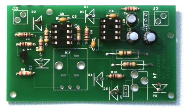
PCB Components
Resistors and Diodes
Step 1: Resistors and Diodes
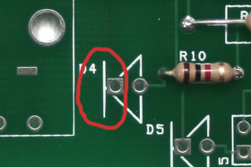
The black line of the diode should go to the side that is circled.
First solder all the resistors and diodes into place. You will need to align the line on the diode with the line that is at the tip of the triangle. Look at the photo to the right to get a better idea of how to place the diode. The resistors are not polar sensitive so you may install them in any orientation.
The placement D1 on the PCB does not have a component and needs to be shorted. Simply use one of the leads that you clipped from a resistor or diode and short the connection on D1.
Capacitors
Step 2: Capacitors
Now solder all the capacitors. The electrolytic capacitors C2, C3 and C6 are polar sensitive. Make sure that the longest lead from the electrolytic capacitor goes into the via that has a round border and the shorter, negative lead goes into the via that has a square border. The ceramic capacitors are not polar sensitive and can be installed in any orientation.
Transistor
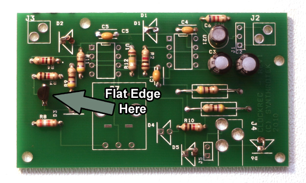
Step 3: Transistor
Make sure to align the flat edge of the transistor to the arrow.
For placing the transistor pay close attention to the photo. The transistor will only function if placed in a specific orientation, placing it backwards will give you a malfunctioning circuit and may damage it. The gray arrow points to the side which has the flat edge of the transistor.
IC Sockets
Step 4: IC Sockets
For the IC Sockets you will want to align the notch on the socket with the marking on the silk screen. To make it easy to solder the socket flush onto the PCB it’s easiest to first solder two opposite corners of the socket and use your iron to heat the corners while pressing the socket down until the socket is flush to the PCB. After that you can solder the rest of the pins and touch up the two initial corner pins as necessary.
Wired Components
Now it’s time to get out the wire clippers and solder all the wired components!
Potentiometer
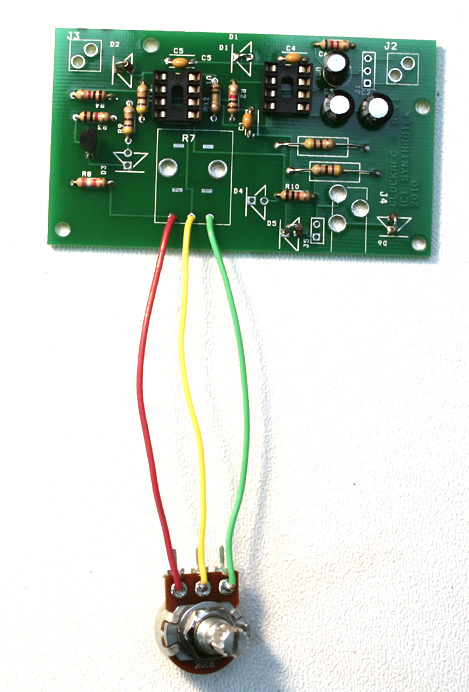
Step 5: Potentiometer
Make sure you wire the contacts from the Pot to the PCB as shown in the photo.
Now for the potentiometer. The pot needs to have each one of its contacts soldered onto the PCB to a specific via. Follow the image above to make sure you are wiring the correct point together.
When installing the pot, some pots come with nubs near the shaft that may get in the way of installing the circuit into a case. Check for a nub and clip as necessary.
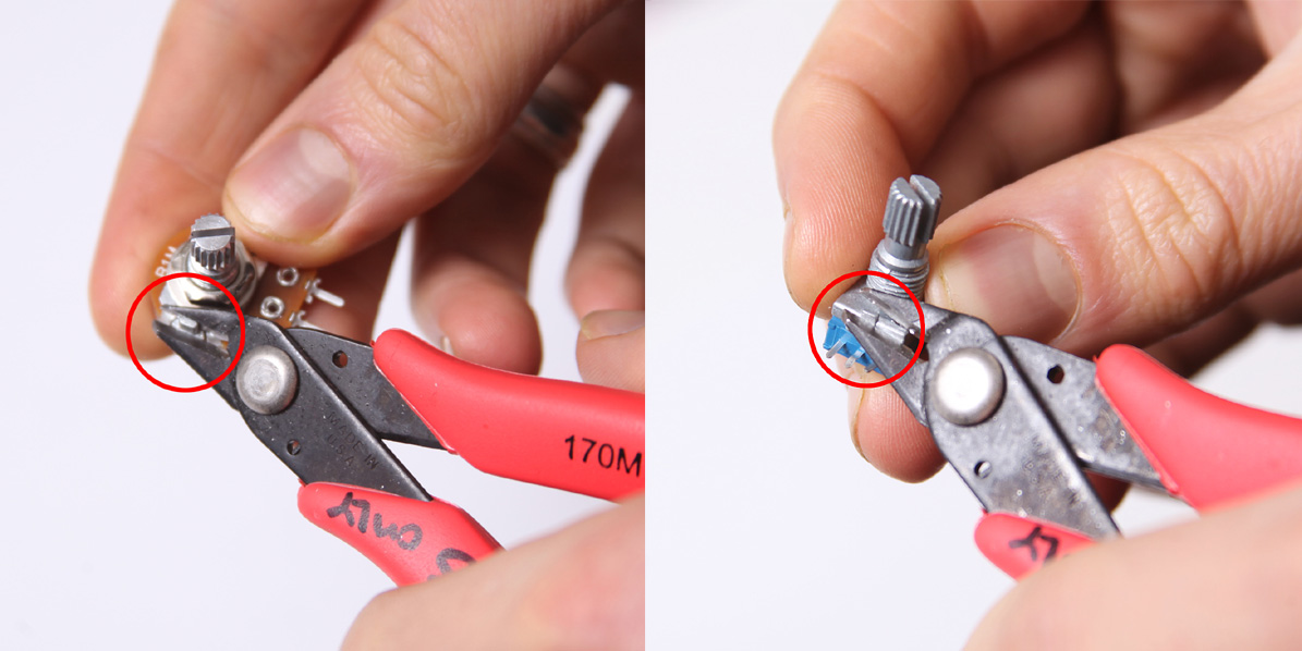
Don’t forget to cut the nubs on the potentiometers as neccesary.
LEDs
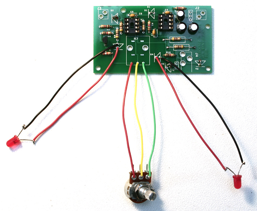
Step 6: LEDs
Next up is the LEDs. The LEDs, like diodes, are polar sensitive and need to placed in a specific orientation. You need to align the flat edge (this is also the shorter lead) of the LED to the line at the top of the triangle in the silkscreen. You can use the same image above that showed the diode orientation if you are still unsure.
Audio Jacks
Mono Audio Jacks
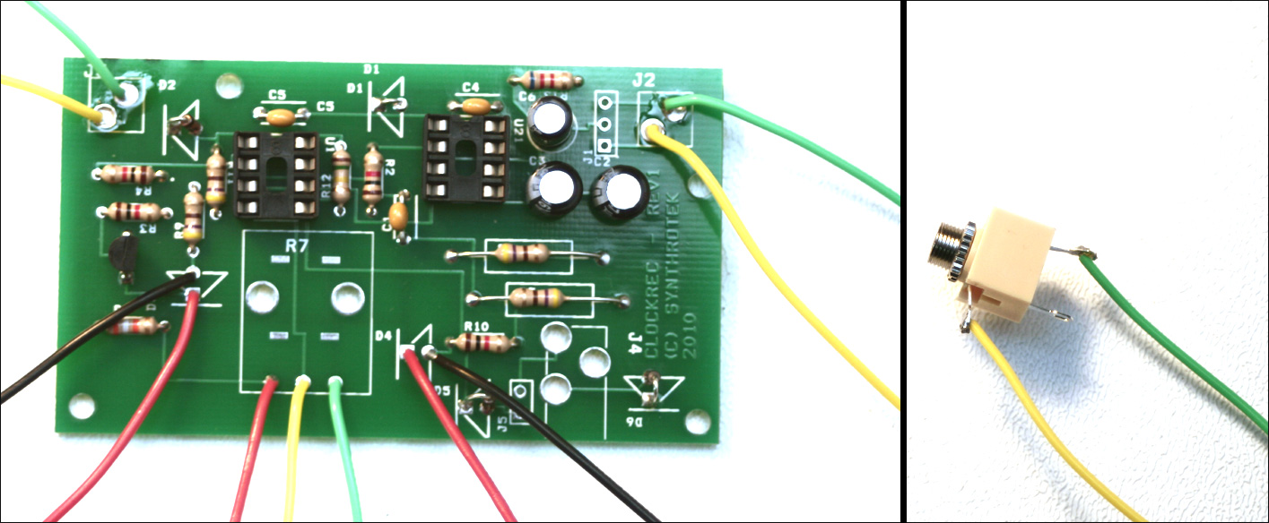
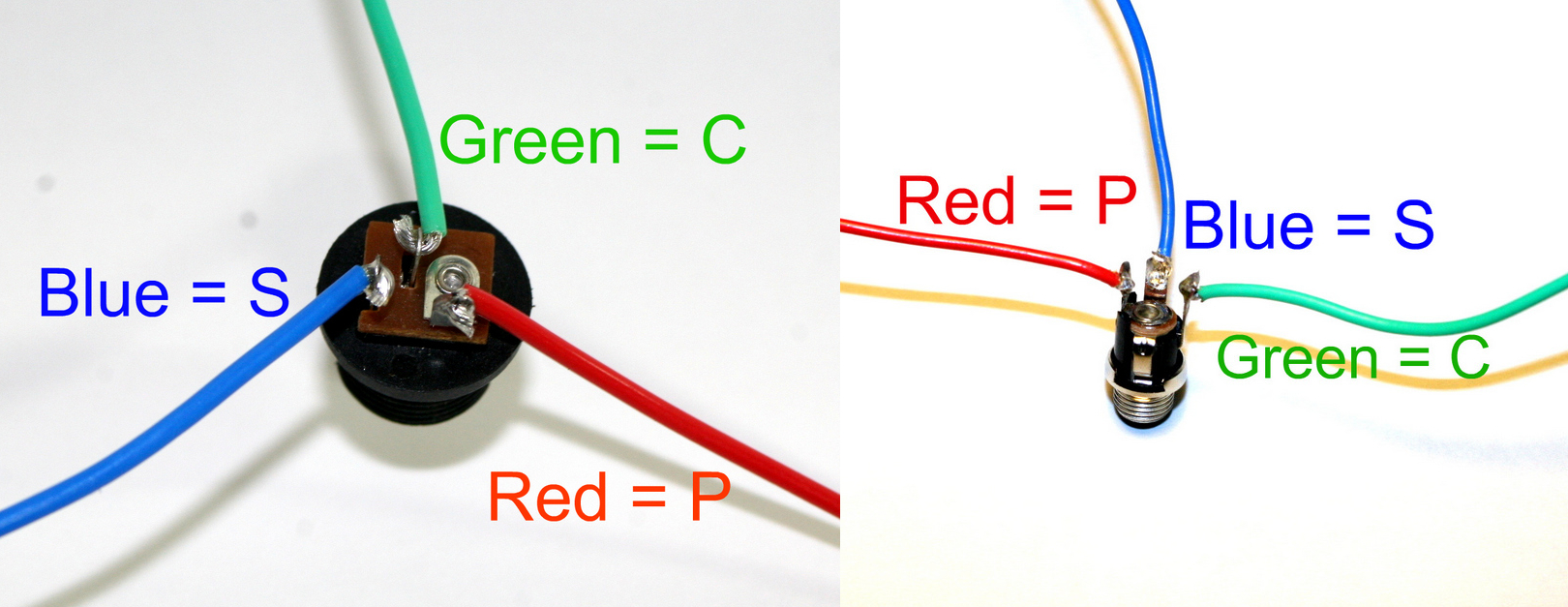
Step 7: Mono Audio Jacks
Use the colored wires as guides as-to how to connect the jack to the PCB.
Since there is no guide on the PCB of which pin on the audio jack goes where you will have to reference the image above to make sure correct wiring. The tip of the jack is marked with a green wire and the sleeve is marked with a yellow wire.
Stereo Audio Jack
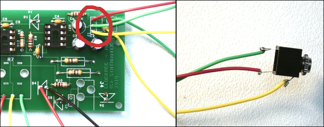
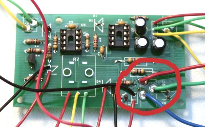
Step 8: Stereo Jack
Like the mono jacks, you will need to reference the image above to determine how to wire the stereo jack correctly. Use the colored wiring connected to the jack and the point on the PCB that is circled in red to determine the wiring for your stereo jack.
Power Connectors
Battery Clip
Because normally this circuit will drain the battery even when no in use we recommend first wiring in a switch on the battery clip to allow you to turn the battery usage on and off. This switch will not be a universal power switch and will not affect the circuit if you have it plugged in via a DC power adapter. Take a look at the image below to get an idea of how to wire a switch to the battery clip. This step is completely optional and you may connect the battery clip directly to the PCB with no switch.
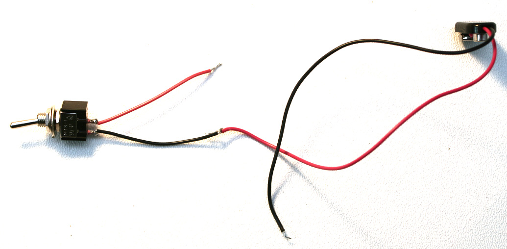
How to wire a switch to a battery clip.
Once your battery clip is ready solder the battery clip to the PCB, using the image below as a guide. Match the black and red wire to their corresponding points that is circled in red.
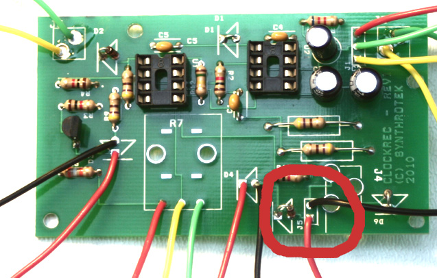
Step 9: Battery Clip
Make sure the red and black wires of the battery clip match the area circled in red.
DC Power Jack
Step 10: DC Jack
Match the wiring in the circle with the DC Jack wiring shown below.
DC Jack Pinout
We’re almost done! For the DC Jack find the DC Jack you received in the 2nd image and match the pins with the colored wires, then look at the image above where the red circle is and match the DC Jack’s pinouts with the wiring shown. And that’s all the soldering to do!
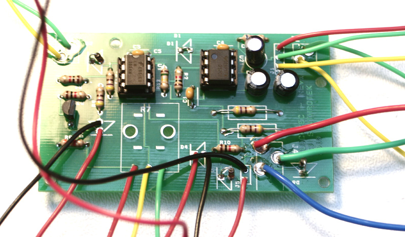
Completed Circuit
Step 11: Install ICs and completion!
Now all you need to do is install the two ICs, making sure that the notch or dot on the IC is aligned with the notch on the IC socket. Plug it in and have fun!