


Welcome to the 10 Step Basic Analog Sequencer Assembly Instructions! This guide will help you properly assemble your circuit. If this is your first electronics project, be sure to go slow and read all of the instructions carefully; this project requires attention to detail when we begin the later stages of assembly.
One of the most important steps in an electronics project is to be sure that you have all of the parts to complete the project. After you identify all of the components, make sure you have the exact number listed in the BOM (Bill of Materials).
BOM Review and Component Identification
PCB


A PCB (Printed Circuit Board) simplifies the construction of an electronics project by having traces and pads embedded into the plastic material along with pre-drilled through-holes. The traces act as wires to connect each component together, the pads surrounding the through-holes allow for efficient soldering, and the through-holes take the guesswork and drilling out of where to place components.
The PCB has two surfaces, top and bottom. The top surface is where a component will be placed and their leads will be inserted through the through-holes. The bottom surface is where our soldering will take place.
ICs

An IC (Integrated Circuit) is, simply put, a miniature circuit that performs a specific function. In our circuit, we have three distinct ICs with three complementary functions. To build the circuit, we only need to be able to identify each IC and where Pin 1 is located.
7555 Timer IC

The 7555 Timer is the heart of the circuit and controls the speed of the clock for the sequence. By using a capacitor/potentiometer pair along with the 7555 Timer, we can control the duration of a sequence step. It has 8 pins for soldering connections. To place the IC properly onto the PCB, see the picture above for the location of Pin 1. Note the half-circle cut-out on the body of the IC; this is a common Pin 1 Indicator. This IC is also commonly referred to as a 555 timer.
TLV2370IP Operational Amplifier

This is what will take our small signal and amplify it. Be careful to differentiate the TLV2370IP from the 7555 Timer, as both have only 8 leads. The cryptic lettering printed on the top face of the IC will have the part ID located somewhere in between the manufacturer’s code. Instead of having a half-circle Pin 1 indicator, this IC has a dot located close to Pin 1 to identify it.
4017 Decade Counter

The 4017 is responsible for the 10 step sequencing of the circuit. They are a lot of fun to experiment with and their sequences are highly modifiable. This IC has 14 leads and the Pin 1 Identifier is a deep half-circle cut-out on the body of the IC.
Resistors

Resistors are color-coded to identify their resistance value, measured in ohms (Ω). If you are new to circuit building or do not have the color codes memorized, here’s a quick cheat sheet to help you identify each resistor used in this circuit:

Potentiometers

Potentiometers are basically variable resistors. They normally have three solder terminals (lugs) where wires can be attached and their resistance values are printed on top (20kΩ for this particular potentiometer).
Electrolytic Capacitor

Electrolytic capacitors are polarized (having a negative and positive lead), meaning that electrical current must flow in one specific direction in order for the component to function properly. To identify which lead is which, note that the negative lead will be shorter than the positive and a gray stripe will be closest to negative lead.
Schottky Diodes

The Schottky diodes in this circuit ensure that electrical current only flows in one direction. These are helpful to avoid damaging sensitive components if a battery or power source is connected incorrectly.
LEDs

Just like the Schottkey diodes, LEDs (Light Emitting Diodes) allow electricity to flow in only one direction, but also emit light when current flows from the positive anode (longer lead) to the negative cathode (shorter lead). The opaque plastic attachment is used to separate the leads from shorting and for mounting into an appropriate LED socket.
9V Battery Adapter

When connected to the PCB, a 9V battery can be connected to this adapter to operate the circuit.
1/8″ Mono Audio Jacks

The mono jacks accept an 1/8″ plug and have three solder terminals, two of which we will use for each input of the circuit. They are used for several functions in this 10 Step Sequencer.
Switches

The toggle switches have two terminals, indicating that they are SPST and only have connected/not-connected (on/off) states.
Wire
You are going to need a lot of wire for this project. Be sure to get multiple colors, as this will make wiring easy to keep track of (red, black, and green are used here). I recommend using thin, stranded wire for flexibility and solid soldering connections.
Assembly
Alright! We’ve identified each component and have all of the parts required for the circuit. This is where the fun begins, so let’s get started!
Notes:
– If you would like to make the basic sequencer, read ahead. If you would like to see the possible modifications to the circuit, check the end of the instructions to see a list of modifications to suit your needs. You may have to de-solder several connections to implement an extra feature if you decide later on that you want a modification to your circuit.
– There are 10 rows of through-holes located near the 4017. This is where the sequence takes place and the majority of the wired components will be soldered to the PCB. The spacing is tight and the wiring is busy, so make sure to take your time and solder carefully.
PCB Components
I suggest starting with components that are soldered directly to the PCB before moving onto wired components, as this keeps the working area manageable and compact.
ICs

Insert the ICs as shown in the picture above. The 555 timer IC is located in the lower left and the TLV2370IP is located in the bottom center.

Be sure to insert Pin 1 of each IC into the square overlay through-hole. Gently squeeze the leads inward if the leads of the IC do not fit into all of the through-holes.
ESD Warning: Be sure to ground yourself before handling the ICs. Some ICs are extremely sensitive to static electricity that your body accumulates and can be damaged by ESD (electro-static discharge). Touch a large metal object or use an anti-static wrist strap to ground yourself and protect your ICs.
Electrolytic Capacitor
The electrolytic capacitor is polarized and proper placement is necessary for the circuit to function.

Note the square overlay in the component identifier overlay – this is where the positive lead (see picture below) of the capacitor will be inserted.

Diodes

The negative lead of the diode is identified by a small black band on the diode’s body.

Insert the diodes as shown in the picture, then solder each lead to the PCB and cut the excess wire.

Resistor

Insert the 10kΩ resistor into the R2 through-holes (see picture above) and solder the leads to the PCB.
We will be adding 10 470Ω resistors to the circuit when completing the wired components stage.
Wired Components
Notes:
– Cut more wire than you think you will need, excess wire can always be cut and the length of the wire impacts where the components can be mounted in a case.
– The PCB’s through-holes are small; be sure to use thin wire (22 / 24 gauge of solid and stranded wire works fine). If the wire you are using is too thick, wrap the wire tighter or remove a couple strands to be able to put the wire into the through-hole.
– Use color-coded wire if you can. Being able to differentiate which wire connects to which component is extremely helpful and time-saving, especially if you plan to modify your circuit in the future (see the Modifications section below).
– The wires in the pictures are long for clarity. If you know that you are mounting your circuit into a small casing, you will most likely want to use shorter wires. Also, I twist my wires to differentiate each assembly and make the instructions easier to follow. This is totally a personal preference.
– A strong physical connection will result in a strong solder connection.
– Any solder connection that is exposed can result in a short when you are mounting the circuit or if the circuit is jostled. I suggest using electrical tape or shrink wrap tubing to prevent this from being a problem.
Timer Potentiometer

Wire three wires of equal length to each of the 10kΩ potentiometer’s solder lugs. Connect these wires to the PCB in the positions shown in the picture above.
9V Battery Adapter
If you would like to add an on/off switch for your 10 Step Sequencer, skip to the Modifications section for instructions on how to wire up an SPST switch as an on/off switch. Otherwise, continue following these instructions. Your circuit will function when a 9V battery is connected to the adapter.

Insert the wires of the 9V battery adapter jack into the PCB through-holes as shown above. Solder onto the PCB and clip the excess wire close to the PCB bottom surface.
CV (Control Voltage) Out


Solder two wires to an 1/8″ mono jack’s terminals. Connect the wires to the PCB as shown in the picture above. You may want to use longer wire than usual, as the CV Out interfaces with external circuits and is not grouped along with the operator controls.

Sequence Steps
Our focus will be on the 10 rows between the TLV2370IP and the 4017 IC, which are the individual steps of the sequence. Each through-hole is numbered in the following diagram:

Positions 7 & 8 are occupied by the diodes placed earlier. Positions 1-4 are in parallel, meaning that a connection to any of these 4 PCB through-holes can be moved to any of the other three. If you are new to building circuits, follow the instructions exactly to avoid confusion.
At this point in the assembly, we are going to be adding components to the sequencer in an order that allows you to add functionality. You can stop after completing any of the steps and have an operational circuit tailored for your specific needs.
Every instruction needs to be repeated for all ten rows of the sequencer.
Potentiometers for CV Step Output Control

Adding potentiometers to your circuit allows you to alter the control voltage output at that step of the sequence. Once you have finished adding all of your pots your sequencer will function. If you care to add LED indicator lights, on/off (per step) switches to vary your beat, resets, or a few other options, please read on.
Solder three wires as shown above. Insert the wires into the PCB through-holes at the positions shown on the diagram:

LED Step Indicator
If you want to see when a particular step of the sequence is activated, follow these instructions.

Attach a resistor to the negative (shorter) lead of the LED. Next, attach a wire to the positive lead of the LED and a wire to the resistor’s other lead.

Wrap tape around the resistor and the exposed wire to prevent shorting the LED, then tape the rest of the exposed wire.


Attach the positive wire to the Position 3, as indicated on the diagram below:


Solder the negative wire of the LED to the potentiometer’s negative (black wire) terminal.
Sequence Step Skip Switch
If you want to remove a step from the sequence while the sequencer moves through its steps, follow these instructions. You can create interesting and rhythmic sequences with this circuit addition.
Here’s a simple diagram for an overview of the PCB insertion instructions:

Now let’s go step-by-step to properly wire our circuit.

De-solder the black wire of the potentiometer from the PCB (Position 9).
Attach two wires to the switch’s solder terminals.
Insert one wire from the switch to Position 9. Solder the black lead of the potentiometer to the other lead.

When the switch is toggled, the step it is soldered to will not be active. The LED will not light and the potentiometer will not affect the Control Voltage at the output.
Jack Reset
If you would like to shorten the sequencer to less than 10 steps, follow these instructions to add a Reset function to your circuit.
Here’s the wiring diagram for this step:

Connect one wire to the mono jack terminal at solder terminal shown in the picture below.

Connect the wire from the jack to the PCB at Position 1 (the square through-hole) of the step row. This is the Step Reset Jack for that step.

This is the wiring diagram for Row 10:

Connect one wire from the mono jack terminal as shown to Position 5 on Row 10. This is the Master Reset (MR) Jack for the circuit.

When you want to use this feature, connect a two-ended 1/8″ plug cable from the Master Reset Jack to the Step Reset Jack. The sequence will advance to the step before the activated Step Reset and restart at Step 1, shortening the 10 step sequence to one before to the Reset.
Once all of the rows have been soldered and the components are groups, your circuit should look like the picture above. You have just finished building your own 10 Step Sequencer. Congratulations! From here, you should test your circuit for proper operation and find a case to mount your circuit into. Also, check out the Modifications section to add new features and enhance the functionality of your circuit.
Testing
Coming Soon…
Modifications
Coming Soon….
Adding an On/Off Switch
One of the reasons I left this as a modification instead of a required part of the assembly instructions is because the wiring is identical to many other circuits using 9V batteries as power sources. You can use this wiring on future circuits that you build. The principal is the same in all: create an open circuit using an SPST switch, thereby preventing the flow of electrical current from one pole to the other.
If you already have attached your 9V battery adapter to the PCB, de-solder the positive lead.
Attach two leads to an SPST toggle switch. Insert one lead to the former positive lead through-hole and solder it to the PCB. Wrap the wire from the 9V battery adapter and the free switch wire together, then solder and tape with electrical tape.
You now have a functional On/Off switch for your sequencer.
Adding an A/C Adapter Jack
9V batteries are not cheap. Accidentally leaving your circuit on when not in use will most likely leave you with a weak or non-functioning circuit. A/C adapters (or wall warts, as they are commonly known) take the voltage from a standard household outlet at ~120V and step it down to a usable voltage.
When choosing an A/C adapter, you must be sure to use the correct voltage and current rating to avoid frying your circuit or not properly powering it. In addition to this, we have to pay attention to how the plug of the adapter is wired. Center Negative and Center Positive refer to the polarity of the barrel plug. On the A/C adapter jack, you will notice a pin in the center. If the solder terminal that connects to this center pin is on the positive rail of your circuit, you will need a correctly rated Center Positive A/C adapter. If the center pin is connected to the negative, it will be Center Negative. There is a standardized marking on most A/C adapters that takes the guesswork out of identifying which connection is which. Using a voltmeter can identify it as well if the Center Pin ID symbol is missing.
More to come soon…
Varying the Speed of the Sequencer
Different potentiometer and capacitor combinations can influence the speed of the sequencer. More on this coming soon…
Adding a Switched External Clock Input
Coming soon…
Sequence Length Limiter
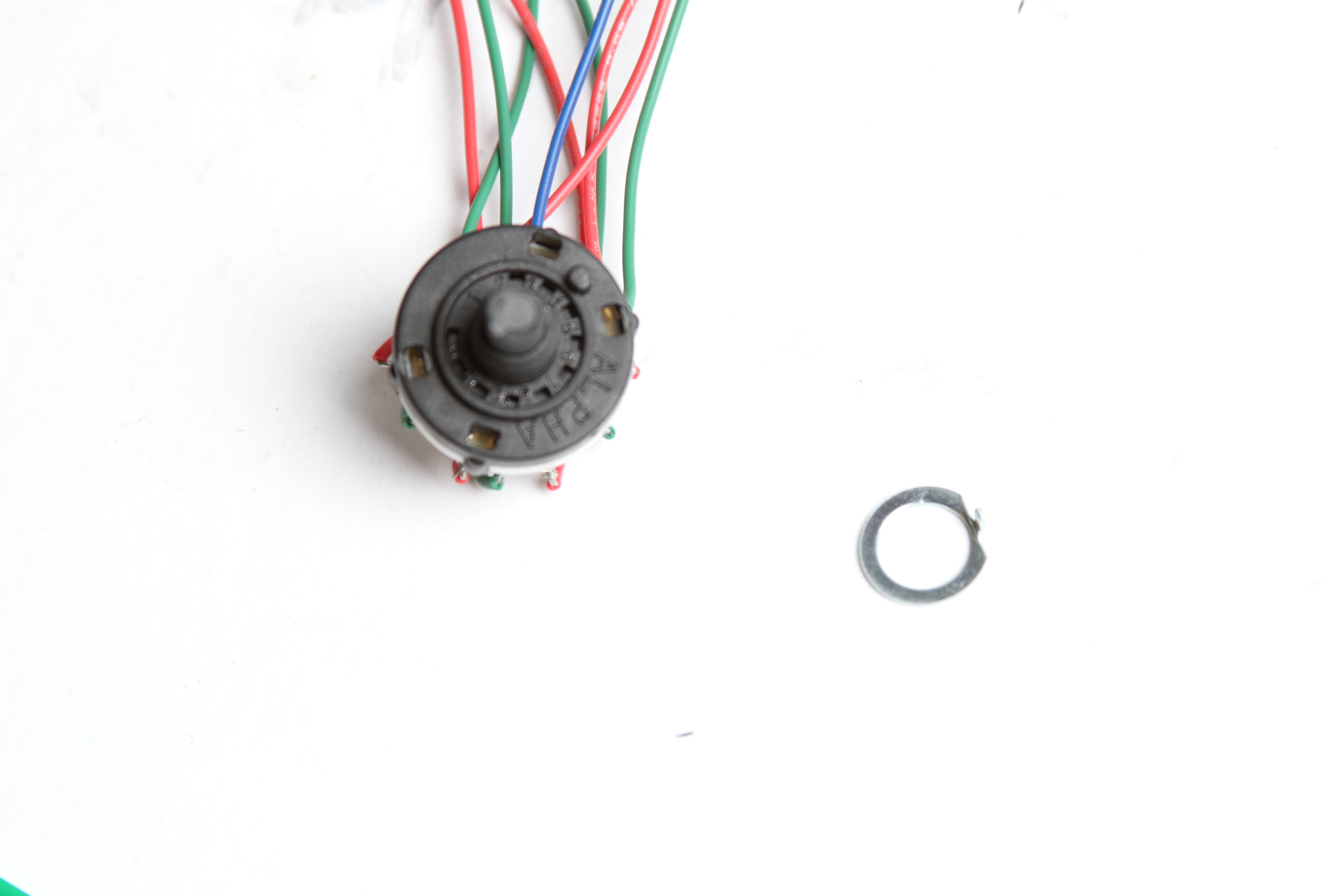
If you’ve already built your sequencer, you’ll notice that your CV sequence is always 8 steps. You may want to limit the sequence pattern down to 4 or 6 steps to sync up with a beat or just repeat a simple pattern. To do it, you’ll need an 8 position switch and a Schottky diode.

Solder wires to each of the solder terminals on the jack. If you look at the switch above, you’ll notice a series of numbers by each solder terminal indicating the switch position. This is important, so I color-coded my wires to avoid mixing them up. The blue wire in the middle is the common terminal.
If you are using a different type of switch, I suggest using a multimeter to test continuity between the common terminal and the switch position terminals.


Because many of these switches are manufactured overseas for a wide variety of uses, there are certain switch terminals that are omitted during construction. However, the shaft of the switch will still rotate into positions 9-12 even if it lacks a solder terminal.
To fix the switch to 8 positions, use the included limiter ring to limit the range of motion for the switch. On this particular switch, insert the tab into the hole to the right of ‘8’. Test your switch to see if it rotates to 8 distinct positions.
Now that your switch is wired up, you are going to attach it to the board.

Looking closely at the board above, you will see a diode connected on step 9 to the reset pin 15 of the 4017 via the 5th position through-hole (trace the leads if you are unsure). This diode limits the possible number of steps from 10 to 8. The 4017 decade counter IC only has 10 individual steps before a reset to the beginning of the sequence, Step 1. In this particular circuit, the diode is acting as a set length sequence safety. With many multi-position switches, the connections from one step to the next are not “make before break”; connections between the common terminal and two switch positions are momentarily open. In a sequencer circuit with a multi-position switch and a fast clock, this can result in the sequencer stepping into invalid steps (9 and 10 in an 8-step circuit). So, make sure you limit your circuit’s sequence when using one of these switches. It really makes this mod worthwhile.

Find the wire attached to the switch’s solder terminal 1. Find the second step’s square through-hole (the 1st four through-holes of each step are connected, so you can use those too) and solder the wire to the board. Continue onward with the next step and switch position wire. It should look very similar to the pictures.

Before soldering the multi-position switch’s common wire to the PCB, attach the Schottky diode to the end. The wire should be soldered to the the diode lead furthest away from the black band (the anode). The remaining lead should be inserted into the same column as the safety diode’s cathode.
That’s it! Now test each step to see if your switch is working correctly. You should be able to switch between 8 sequence lengths.
One of the best parts of this mod is that it gives you the ability to tune each step’s particular output voltage. Turn the switch to position one and tune. Turn to the next step and hear your sequence being built. Continue until you get a rad sequence!
The link to the exact materials page doesn’t work! Out of curiosity about how much would it cost to get all the materials necessary to make this and is it too difficult of a project for a novice to take on?
Check out this link, it is working here, thanks!
http://www.synthrotek.com/kit-assembly-instructions-2/
This kit has a lot of wiring, it is not super hard, but you may wanna get your soldering skills up with a smaller/cheaper kit.
Thank you!
Hello, is there any replacement for tlv2370?
I broke …….
Greetings, thanks.
we can get you a new one if you like, please email synthroteksales@gmail.com