


Important Links
Store Page
Assembly Instructions
Bill of Materials
Operating Instructions
Schematic
Case Drawing
Capacitor and Resistor Lookup Guide
Attention: This is the FORMER version of the Voice of Saturn Sequencer build instructions; it does not include the Mod kit. If you like, you can purchase the Mod kit HERE. There’s a new set of instructions that includes the Mod kit and an optional panel HERE.
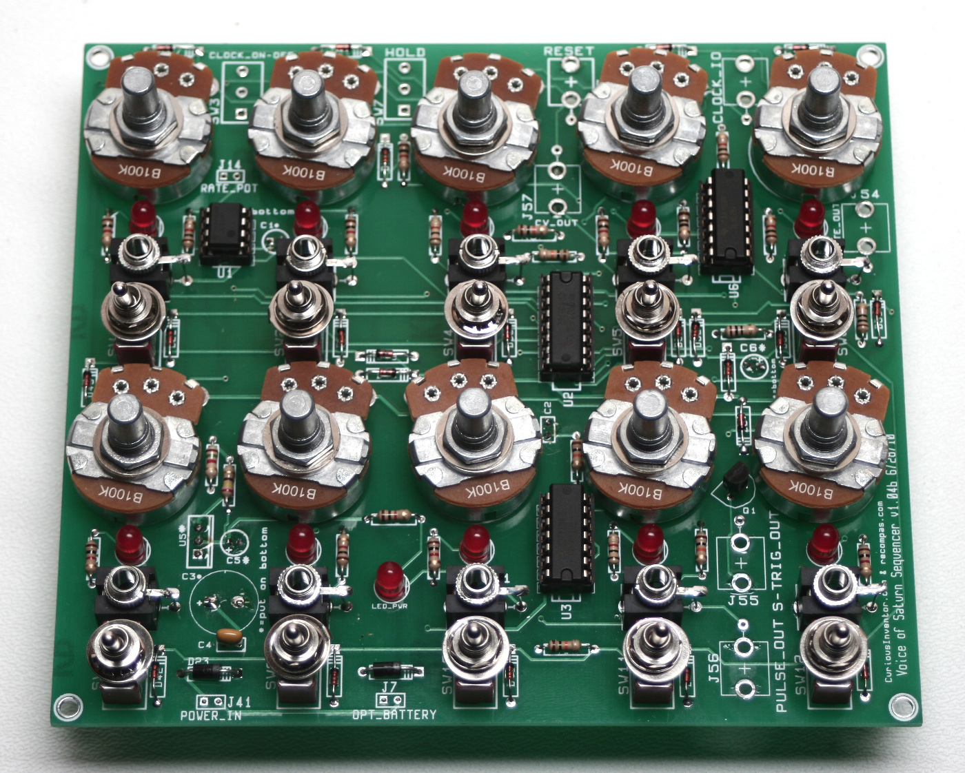
Welcome to the Voice of Saturn Sequencer assembly instructions! This guide will walk you through the process of assembling your ten step analog sequencer.
BOM Layout
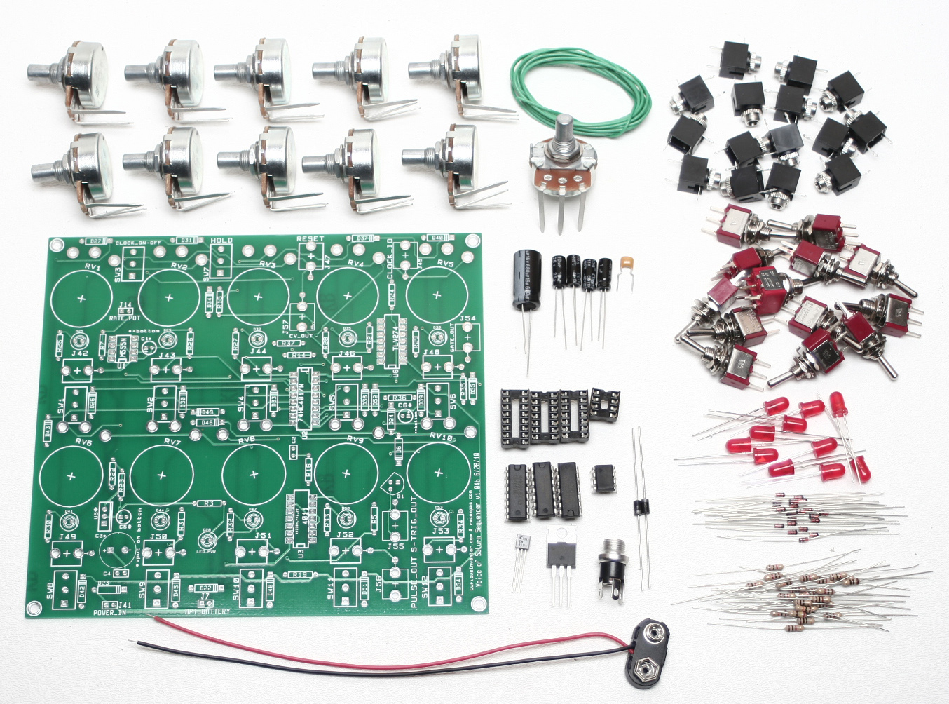
Check your kit against the BOM and verify that all components are present – if anything is missing we will ship it to you free of charge.
Attention: Changes may occur after the Assembly Instructions are created and the photos may not reflect those changes. Always use the BOM to verify the placement of components.
Resistors
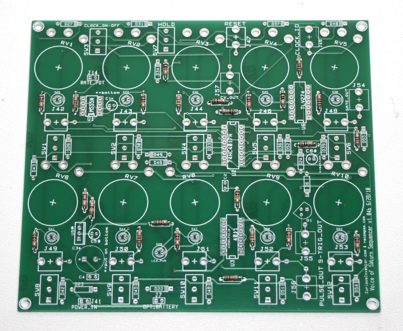
Begin by soldering all resistors into place – resistors are non-polar components and may be inserted in any orientation.
Diodes, Sockets, Transistor, & Ceramic Capacitor
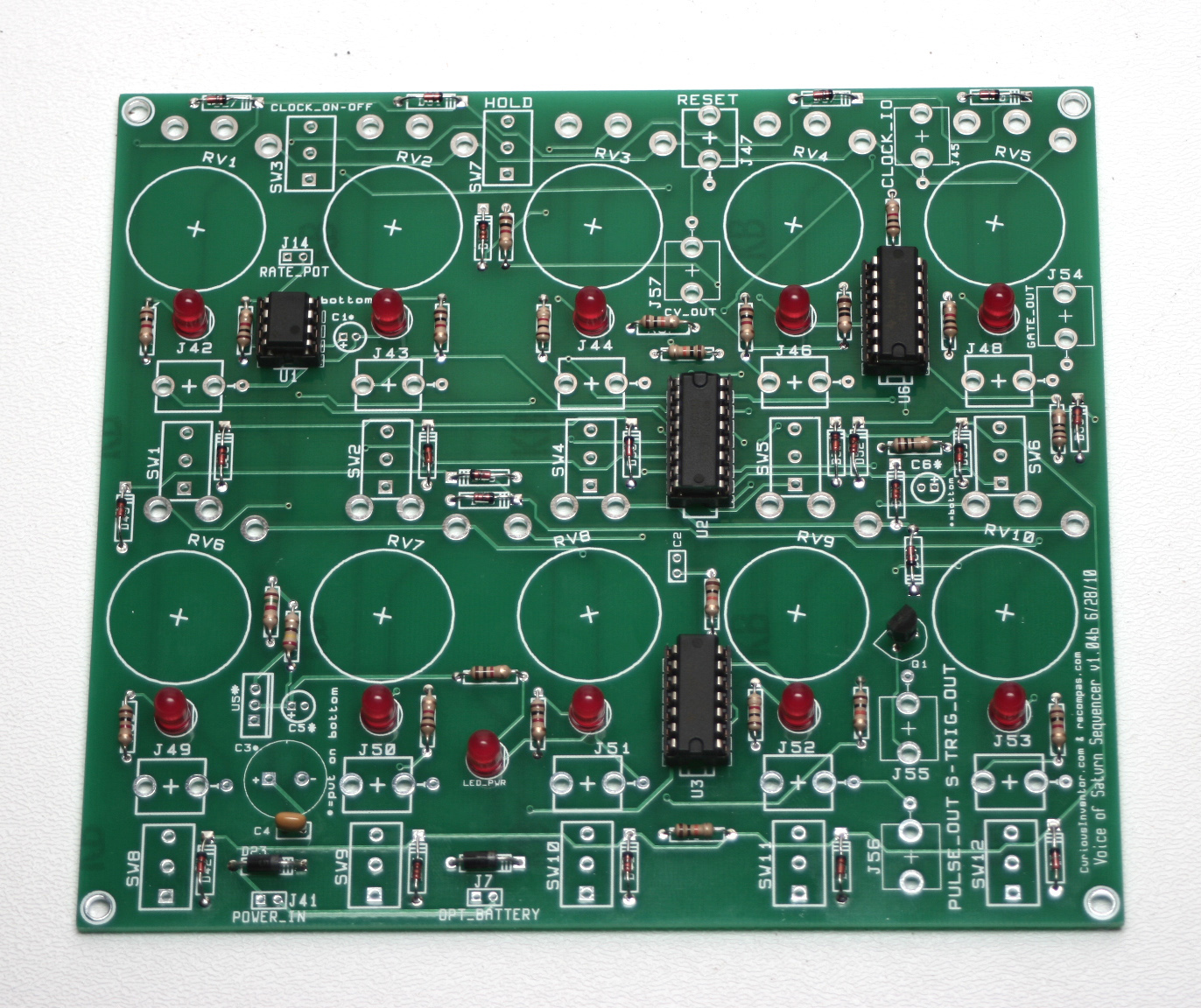
Next install the sockets, diodes, transistor, and ceramic capacitor. Align the flat edge of the LEDs and the polarity stripe on the diodes to the corresponding markings on the silkscreen – orient the transistor (Q1) in similar fashion. The ceramic capacitor (C4) is not polar and may be installed in any position.
Electrolytic Capacitors & Voltage Regulator
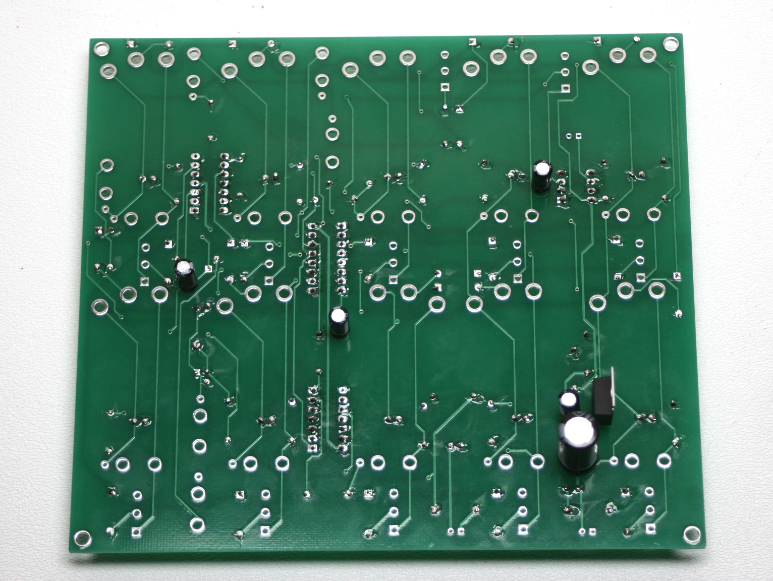
Install the voltage regulator and electrolytic capacitors on the back of the board using the above photo for reference orientation. The polarity markings for the capacitors on the opposite side of the board are correct, but the voltage regulator *must* be oriented opposite the direction indicated by the silkscreen when installed on the back of the board. It is not necessary to place the capacitors and voltage regulator on the back of the PCB if you are not intending to install the circuit in a case.
PCB-Mounted Pots, Jacks, and Switches
Next solder all remaining PCB-mounted components into place. The SPDT switches have a very snug fit and may require above average force when inserted through the board vias. It may be necessary to remove nubs from the potentiometers in order to install the circuit in a case:
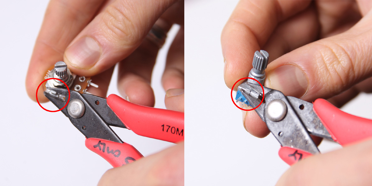
Don’t forget to cut the nubs on the potentiometers as necessary.
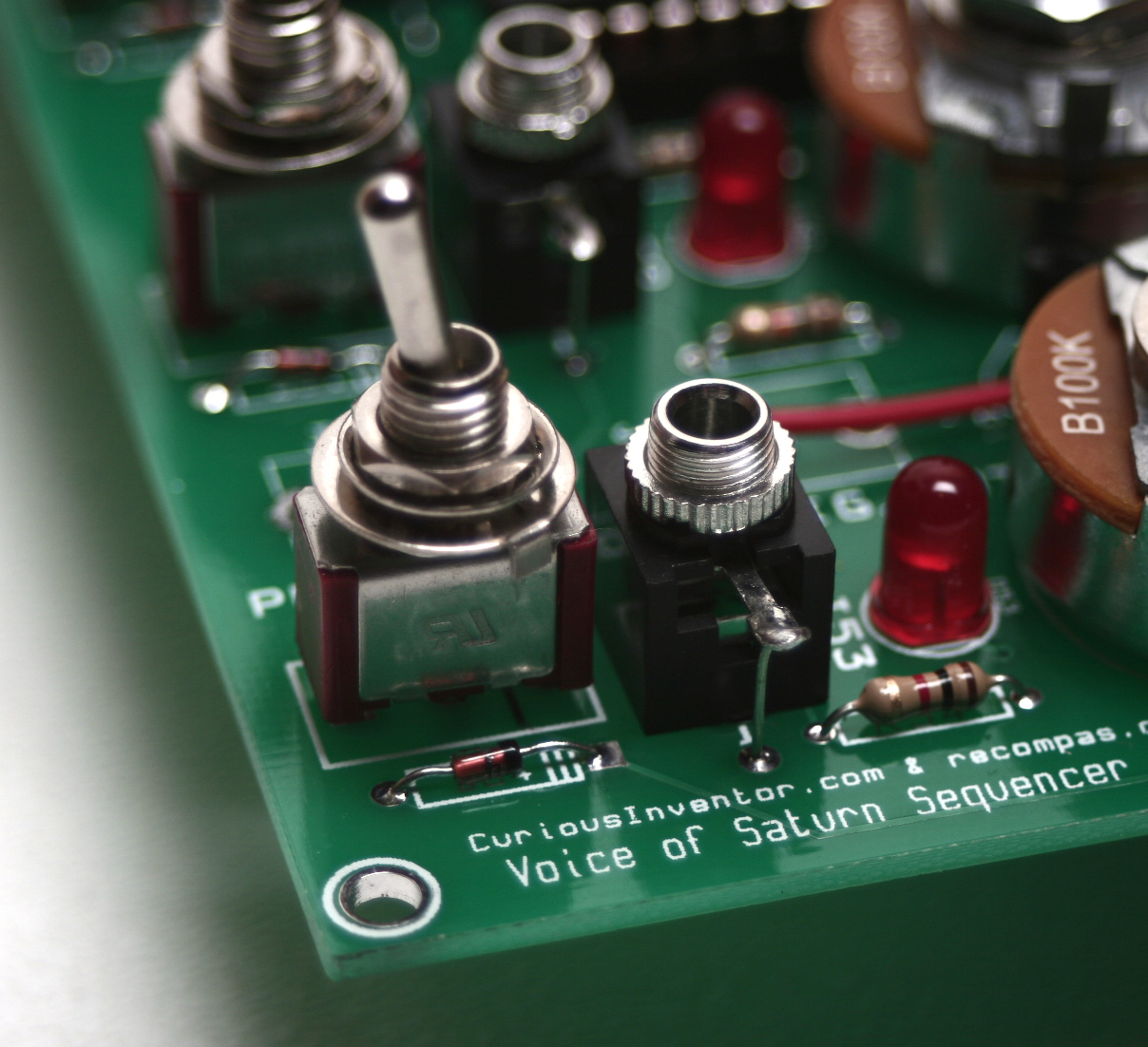
Solder all three contacts on the 1/8″ mono jacks to the board utilizing clipped leads to connect the sleeve contact to the board:
Wired Components
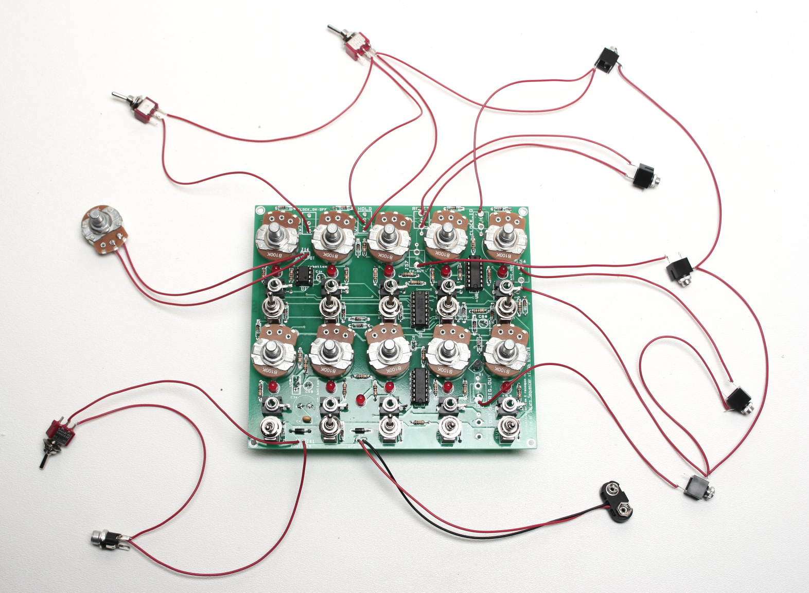
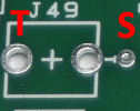
Solder leads to the remaining components and connect them to the board using the above photo for reference. There are a number jacks that must be connected together in order for the circuit to function properly. Only pins 2 and 3 are connected on the rate pot (J41) – solder pin two to the circular via and pin three to the square via. Do not connect the sleeve/gnd contact perpendicular to the tip contact on J47 (RESET).
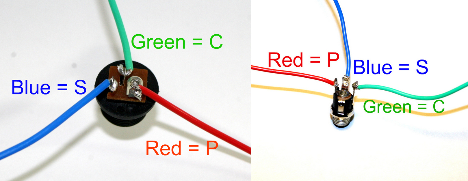
DC Jack Pinout
For 9V center negative: connect the positive lead on the DC jack (S) to the square via and negative lead (P) to the circular via on J41, respectively – a SPDT/SPST switch may be soldered in line with the positive lead to act as a power switch. The 9V battery connection (J7) is optional and follows identical polarity orientation to J41. A SPDT/SPST switch may also be connected in line with the 9v battery connector if desired:
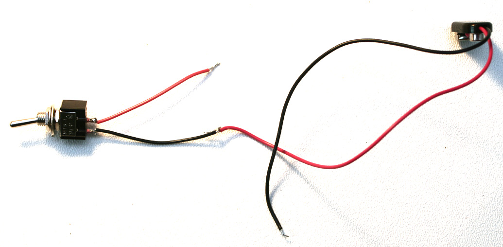
How to wire a switch to a battery clip.
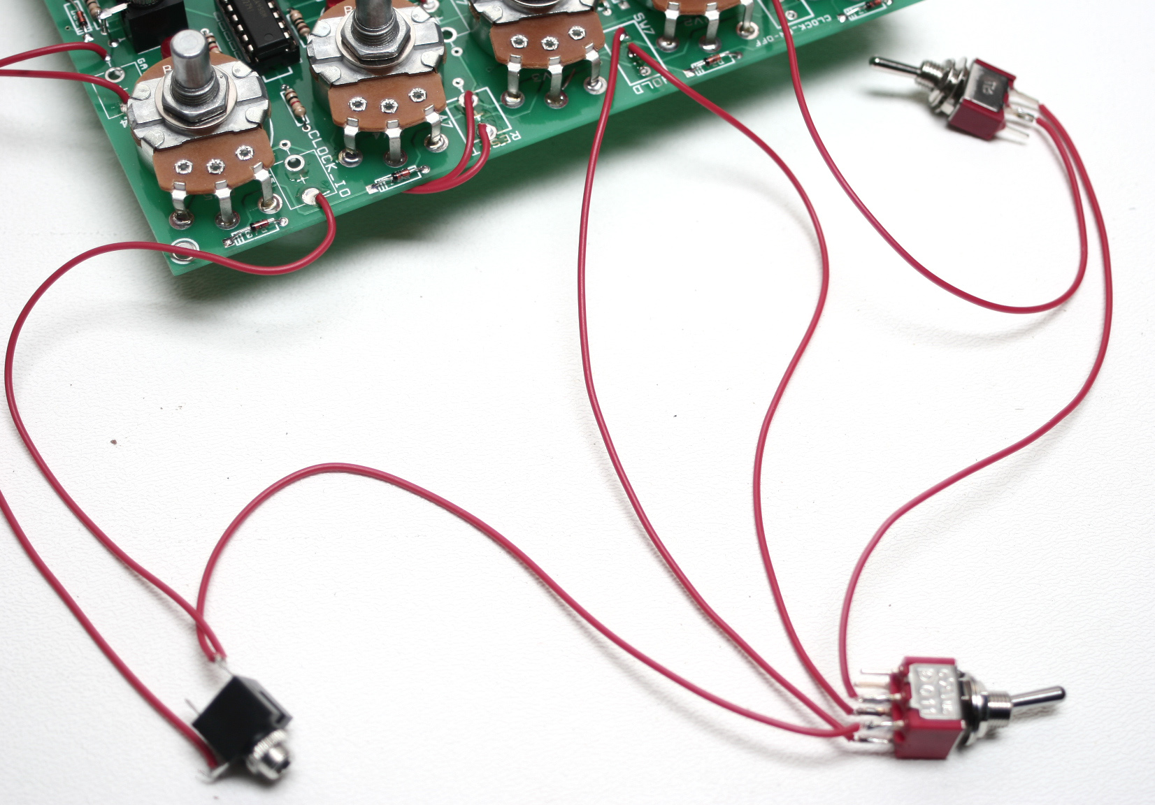
The hold and clock on/off switch wiring is particular confusing, and the following photos provide a closer inspection of the correct wiring:
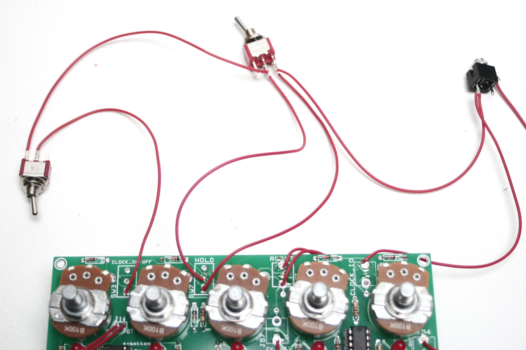
Connect the center contact of the SPDT switch to the square via of SW3 (CLOCK_ON_OFF) and one of the remaining outer contacts to a center contact on the DPDT switch. Solder a lead from one of the adjacent outer contacts on the same side of the DPDT switch to the tip connection on the CLOCK_IO jack (J45). Connect the middle contact on the opposite side of the DPDT switch to the center via of SW7 (HOLD). Connect the remaining outer contact on the DPDT switch adjacent to the contact soldered to the CLOCK_IO tip to the square via on SW7 (HOLD).
Your sequencer is now ready for testing!
WARNING: Never connect a 9V battery and D/C power adapter simultaneously or input an external clock signal to the sequencer with the internal clock enabled – doing so may damage the circuit!
Having trouble connecting wired components? Check the original front panel wiring diagram for more information – this applies to version 1.04b (current) as well.
If you are using 1/4″ jacks without a shunted third contact, follow this connection diagram for all jacks barring J47 (RESET). Tip/sleeve connections correspond identically for all jacks wired directly to other jacks and switches.
i don’t see any pictures on here of what it would look like with all the jacks soldered onto the board directly. do you have a drill template for that?