


Welcome to the LoFi Fuzz Distortion Kit Assembly Instructions! This circuit is an easy build and you’ll be done in no time at all. Let’s get started!
BOM Layout

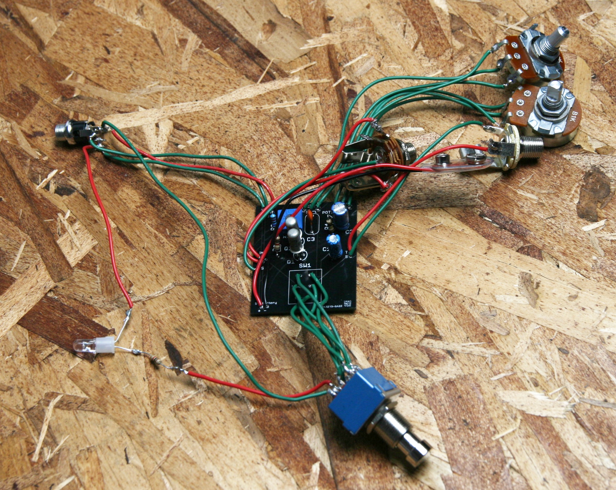
Before starting any successful electronics project, it’s a good idea to lay out all of your parts and make sure that you check it against the BOM. If you are missing anything from your kit, we’ll send it to you free of charge.
Alright, now that you have all the parts, let’s get started building our circuit!
PCB Components
We start with the components that are soldered directly to the PCB. Doing so keeps the working area small and manageable. We’ll be adding the wired components later.
Resistor/Diode/Transistor

Find the silkscreen identifier R1 located on the top of the PCB. Insert the leads of the 10kΩ resistor into the through-holes and solder the component to the PCB.
The diode D1 is a polar component, which means that you will have to be careful about which lead goes into which through-hole. If you look closely at the body of the transistor, you will notice that there is a thin black band next to one of the leads. That is the negative lead of the diode. The silkscreen identifier for D1 has a vertical white band next to a square through-hole. This is where the negative lead of the diode will be inserted.
The transistor Q1 is easy to place onto the PCB. Note that the transistor’s body has a flat side while the rest is circular. If you look at the silkscreen identifier on the PCB, you will notice that the shape is similar to the transistor body. This is exactly how the component will be placed onto the PCB. You will most likely need to spread the leads out a bit to get the component to fit. You don’t need to have the transistor flush against the PCB; leave some space between the body of the transistor and the PCB.
Capacitors

C1 and C2 are non-polar capacitors and their leads can go into either hole designated by the silkscreen.
C3, however, is a polar electrolytic capacitor and needs proper placement for the circuit to function. On most electrolytic capacitors, there is a color band along the body. The lead closest to this band is the negative lead. Also, the positive lead will be longer than the negative lead. On the PCB, the silkscreen for C3 has a tiny ‘+’ next to a square through-hole. This is where the positive lead of the capacitor will go. The negative lead will be inserted into the circle through-hole.
That’s all of the components that are soldered directly to the PCB. Our next step is to use wire to attach the rest of the components.
Wired Components
Potentiometers

Our first wired components to attach to the PCB are the potentiometers. On the PCB, they are labeled as ‘Fuzz’, ‘Thickness’, and ‘Volume’. ‘Fuzz’ and ‘Thickness’ are 10kΩB potentiometers and ‘Volume’ is a 100kΩA potentiometer.

On the PCB silkscreen for all of the potentiometers, there are numbers close to the through-holes. These identify where wires that are attached to the potentiometers are inserted into the PCB.

We suggest attaching wires to the potentiometers first rather than to the PCB then to the potentiometers. Wire can always be clipped if it is too long; having to solder extra wire to too-short PCB-soldered wire is an extra unnecessary step.
Power Jacks

The circuit uses two separate power supplies, a 9V battery adapter and a DC Jack.
The 9V battery adapter is easy. Connect the red wire to the square through-hole on the PCB marked ‘+’ . Connect the black wire to the circle through-hole marked ‘-‘.
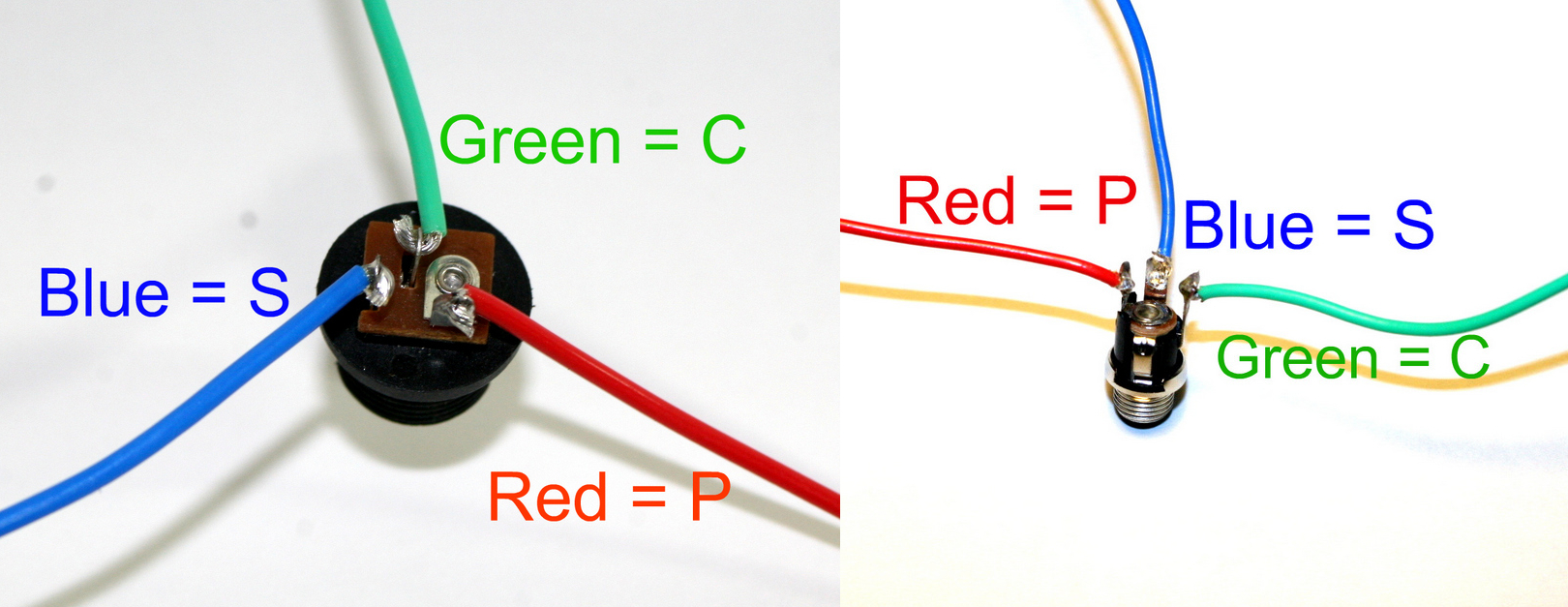
DC Jack Pinout
The DC jack requires a little extra attention. On the board, the ‘DC Jack’ silkscreen has a ‘P’, ‘C’, and ‘S’. These should match up with the DC Jack’s wires (see picture above).
If you do not want to install the 9V DC jack and only install the 9V battery clip you will have to short the S and C pins for the 9V DC Jack like shown in the picture below*.
* Your PCB may not look exactly like the photo, that is ok. What is important is that you short the same pins as shown in the photo.
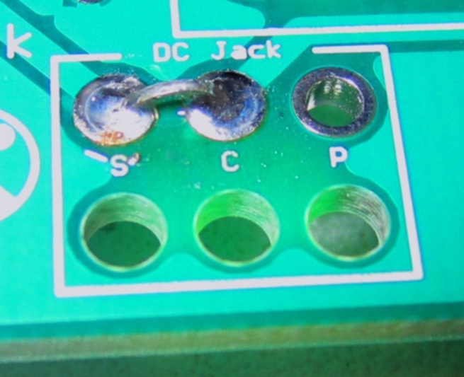
Short these contacts to get the circuit to work without the 9V DC Jack
DPDT Switch/Audio Jacks

Align the DPDT switch’s solder lugs with the PCB through-holes for SW1. This is how the wires will be attached to the PCB.

When the switch is pushed, the input signal will switch from a clean signal to a distorted signal that is processed through the circuit.

Locate the silkscreen labeled ‘In’. There are three labels next to it: ‘T’ for Tip, ‘R’ for Ring, and ‘S’ for Sleeve. These connections are for a stereo jack input. If you are unfamiliar with the solder lugs on a stereo jack, see the picture above. The solder lug directly beneath the Tip solder lug is not used in this circuit.
In this configuration, power will be used by the circuit only when there is mono plug connected to the jack (especially useful with a guitar, which normally uses a mono signal).

The ‘Out’ jack has only two solder lugs and is easy to connect . Connect the Sleeve wire from the jack to the ‘S’ circle through-hole and connect the Tip wire from the jack to the ‘T’ square through-hole.
That’s it! Congratulations on your very own hand-made LoFi Fuzz Distortion! Keep coming back to these instructions, as there are several ways to modify the circuit for different sounds!
Mods
LED Bypass Status Indicator
This mod allows you to have an LED turn on when the circuit is active. When you press the bypass switch, the input signal will bypass the circuit and the LED will turn off.
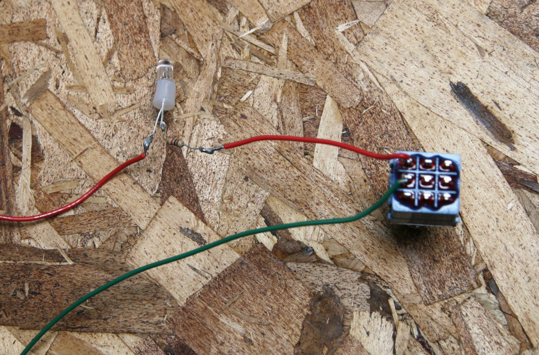
You will need a 3PDT Switch, a 1kΩ resistor, and an LED.
If you have already constructed your circuit with a DPDT switch, remove it from your circuit. The 3PDT switch will replace its true bypass function while also switching the LED on/off.

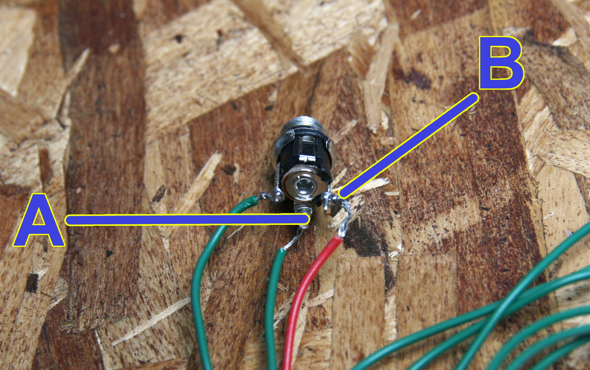
Orient the switch so that the solder terminals are horizontal. In the above diagram, the solder terminals on the switch and the through-holes on the PCB for SW1 are labeled for clarity Terminal C is not used for this circuit.

Attach two wires to terminals A and B on the 3pDT switch. Connect a resistor to terminal A’s wire. On the LED, the body of the LED will have a flat side – the lead nearest to this side is the negative lead, the longer lead on the round side of the LED is positive. Connect the negative lead of the LED to the resistor. Connect another wire to the positive side of the LED.

The resistor-LED assembly from terminal A connects to the Sleeve terminal of the DC Jack. The wire from terminal B goes to the Pin connection of the DC Jack.
The last step is to match the wires from the PCB at SW1 to the 3PDT switch (use the diagram above).

Congrats, you’re done!