


Important Links
Product Page
Store Page
Assembly Instructions
Bill of Materials
Schematic
Capacitor and Resistor Lookup Guide
Welcome to Synthrotek PT2399 Dev Delay Assembly Instructions! This step-by-step guide will take you through the whole circuit-building process.
Component Layout
The first step in any successful DIY electronics project is to make sure that you have all of the parts and know their reference ID for proper board placement. Check the contents of your kit against the BOM before you begin. If you’re missing anything, send us an email and we’ll get it out to you ASAP.

Got all of your components? It’s time to start building.
Assembly
The first part of our build will be for components that are soldered directly to the circuit board. This makes the build process easier than having to deal with wires and floating potentiometers getting in our way while we solder sensitive components.
Attention: Changes may occur after the Assembly Instructions are created and the photos may not reflect those changes. Always use the BOM to verify the placement of components.
IC Sockets/Resistors

Insert the resistors into their respective PCB positions and solder them to the board. Use the BOM to identify resistor placement. Don’t worry too much about damaging resistors with your soldering iron; resistors are not fragile components.
Insert the IC Socket into the PCB as show above. Make sure that you align the notch on the socket with the notch on the silk screen. Next place the IC into the socket as well and again align the notch on the IC with the notch on the socket. Do this carefully as to not bend the IC pins.
Capacitors

There are two different types of capacitors in this circuit. Electrolytic capacitors (C2, C3, C9, C13, and C14) are polar components and their pcb placement matters. The shorter lead and the band on the body identifies the negative lead, which will be inserted into the circle through-hole. The positive lead will be longer and should be inserted into the square through-hole.
Polarity is not an issue with the remaining ceramic capacitors. Just be sure the component values are identified before soldering them; some of them look very similiar and the codes printed on their bodies are the only way to identify them.
Note: (C15, C17) could be either electrolytic or ceramic capacitors.
Voltage Regulator

Solder the voltage regulator for U2 as shown in the picture. Align the flat side with markings on the board.
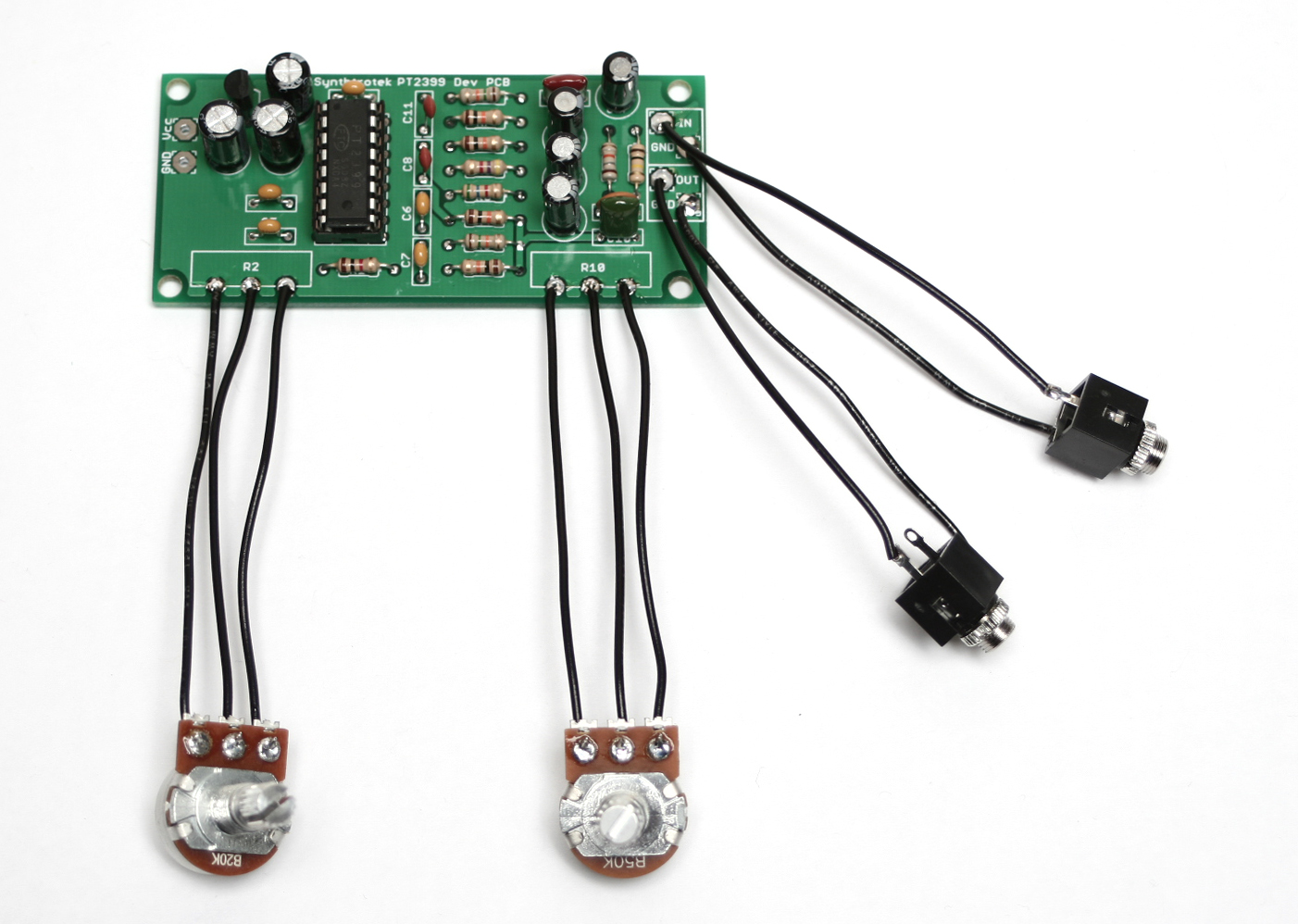
Potentiometers & Audio Jacks
Solder wired leads to a B50K potentiometer, B20K potentiometers, and both audio jacks. Connect these components to their respective locations using the photo below for reference.
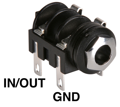
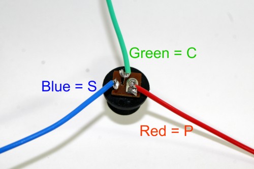
1/4″ Jack Wiring

1/4″ Metal Audio Jack Wiring – Sleeve is Ground, Tip is IN/OUT
You may opt to mount R2/R10 directly to the PCB, but be aware that this will cause the potentiometers to increase mix/depth when turning counterclockwise.

Some pots come with nubs near the shaft that may get in the way of installing the circuit into a case. Check for a nub and clip as necessary.
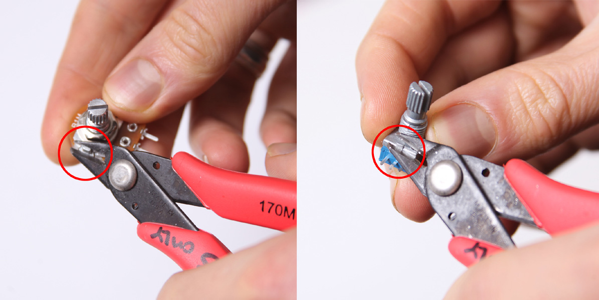
Don’t forget to cut the nubs on the potentiometers as necesary.
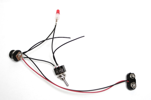
DC Jack, Power Switch, LED, and 9V Clip
For 9V center negative wiring, connect the ‘S’ contact of the D/C jack to one of the contacts on the SPST switch – this switch will control current flowing to both the circuit and power LED. Solder a 1K resistor to the positive (round edge) lead of the LED. Solder two wires to the unused SPST switch contact, connecting one to the remaining contact on the 1K resistor. Solder two wires and the negative lead on the battery clip to the ‘P contact of the D/C jack, connecting one of the two wires to the negative (flat edge) lead of the LED. Connect the remaining wire running from the SPST switch to the ‘VCC’ contact on the delay, and the remaining wire from the ‘P’ contact to the ‘GND’ contact on the delay. Solder the positive battery clip lead to the ‘C’ contact on the DC jack. You may optionally omit the 9v battery clip if desired.
DC JACK WIRING – DEV DELAY
DC Jack Pinout
Warp, Feedback, and Feedblast Mods
Solder wires to both contacts on one of the momentary switches and solder a 200k resistor to one contact on the other momentary switch. Attach wires to the resistor, remaining contact on the momentary switch, and pins 2/3 on the 50k potentiometer. The momentary switch with the resistor will be used for the feedblast mod, the other momentary for the warp mod, and the 50k pot for the feedback mod.
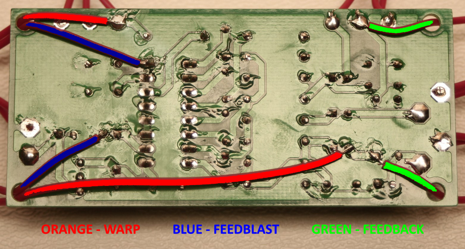
Connect the appropriate components to the following locations:
Feedback: R10 (2) –> 50k pot (2), R11 (via adjacent C17) –> 50k pot (3)
Feedblast: Pin 8 (IC Socket) –> C3 (-)
Warp: R2 (1) –> C15 (-)
Pin 2 on the 50K feedback pot must be connected to pin 2 of R10, and the momentary switch with the 200k in-line resistor should be used for the feedblast mod. Switch polarity has no effect on the feedblast or warp mods. It may be beneficial to route wires through the holes in the corners of the board to provide strain relief for the delicate mod connections.
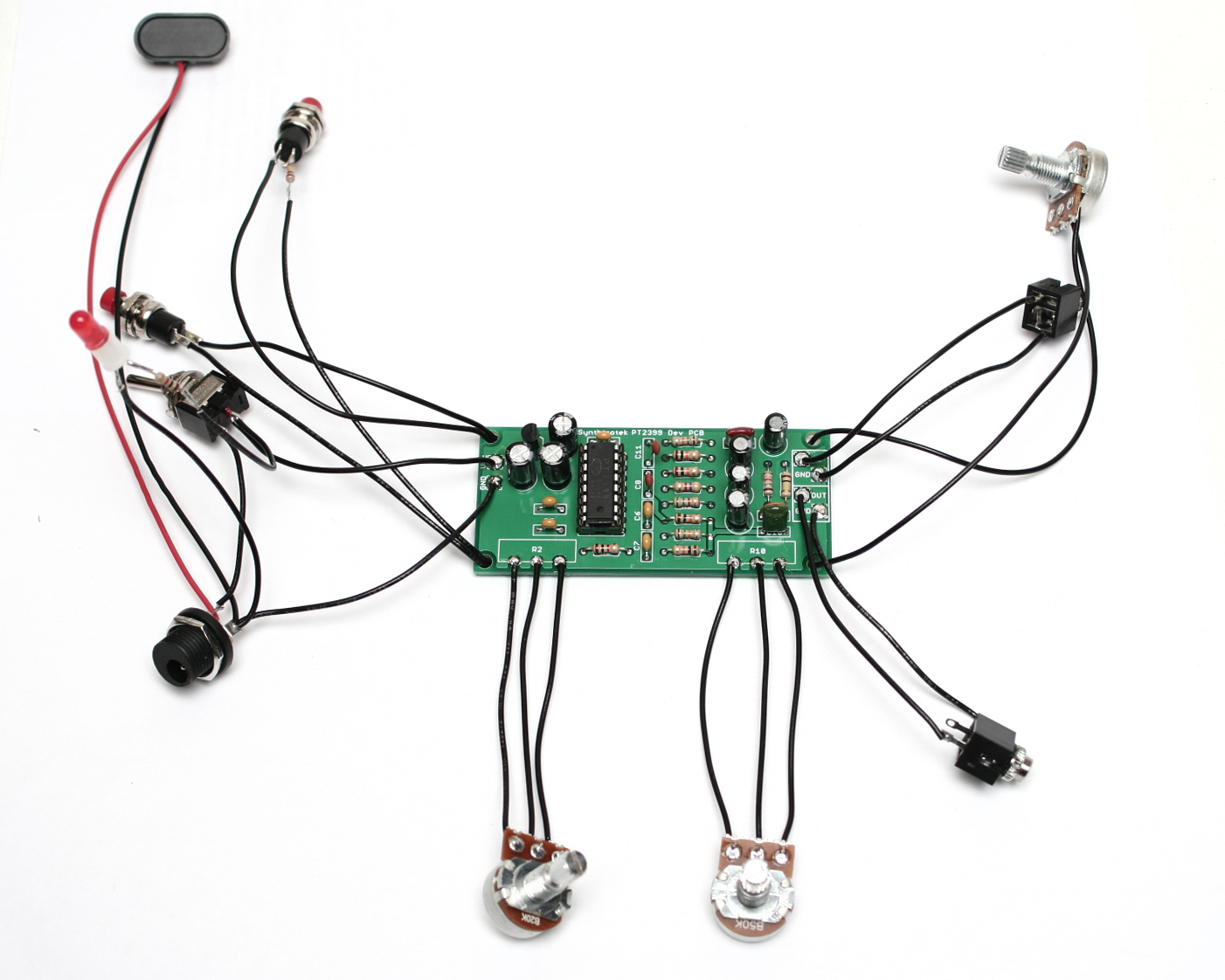
Completed Project
Alright, so the BOM says for C3, it’s a 1 nF ceramic capacitor, but these directions say polarity matters on C3 and that isn’t a ceramic capacitor in the picture. Which is it?
Hmm, perhaps I am missing something, but the BOM I am looking at has:
17 2 C3,C9 47uF Electrolytic Capacitor
Perhaps that is old?
This is a neat kit, simple and clean build. I am curious about whether I should be expecting drop in output volume, though. I’m running a Korg Monotron through this and into headphones and the signal is very faint. The Monotron output through the headphones it as expected, but volume out of the delay board is maybe only 10% (powered by a 9v battery). Is the part of the build and should I plan on amplifying, or did I mess something up?
Hmm, I have not tried many of out kits with headphones, do you have the same experience with an amp?
I’ll try it through an amp and see what things are like. Since you haven’t seen this, it seems like the amount of signal loss suggests I probably did something wrong so I’ll go back and double check everything. Thanks!
@Dave Dave – This project is not buffered, so I would expect some change from the input signal to the output on the delay, I have not checked out how much
@Steve Harmon
Thanks, Steve! As it turns out, it was just a stupid user error on my part. I wound up using 3.5mm jacks that I had on hand that were stereo, but using mono connection to a single speaker. I just needed to bridge the left/right signals and voila! it works just fine. There may be some loss, but it’s not significant like I was hearing last night. Also, running it through a small amp, it sounds just great. I’ll see if I can’t make a recording/vid of this little set up and send it to you if you’re interested in seeing/hearing it.
@Dave Stoked that it is working! I would love to see videos of what you have made.
Hello i was looking at this pcb and it looks different then the other one listed somewhere else on this site.
The other one seems to come with a extra ic and this one does not.
Would this one be able to run like a guitar pedal with true bypass running through it?
Hi Jon,
Which other PCB did you see? It could have been our discontinued stomp-switch based Delay board.
If you wired in a 3PDT stomp-switch between the IN and OUT jacks and the PCB you could add true bypass, though because the circuit is not designed around a stomp-switch you may get some noise in your circuit when you hit the stomp switch.
Anyone know how to get rid of the dry signal on the output?
I found that you can tap the delay only signal from R9. Now i’m feeding that back to the input for more feedback.
Hello.
Can a LM7805 be used in place of the LM78L05?
Thanks!
Hi Rob, this should work, the LM7805 is rated for higher amperage, but should cause no issue
Hi there I’m having huge trouble finding a 3.9nf ceramic capacitor over here in the UK and was wondering if there is any other value capacitor I can use in it’s place?thanks
Hi Paul, try this:
581-AR155C392K4R
3900pf
at UK Mouser
@Steve Harmon
Thanks for the reply,that’s great and UK Mouser is good if I’m doing a big order but too expensive on postage on small orders. Would there be big issues if I were to use a 3.3nf instead?
@Steve Harmon
Thanks sir! Works great! Sounds great!
The LM7805 that is. I had 20 of them on hand.
Awesome PCB, saved lots of time!
One minor suggestion though: you might want to label the connection pads Battery + and Battery – instead of Vcc and GND, since some people may be using this as part of a larger circuit where battery negative and ground are not the same thing.
I’ve built mine into an early ’70s mixer enclosure along with a Music From Outer Space Noise Toaster. It looks like this: http://imgur.com/4RKmEvG
Thanks for the suggestion! Man that case looks superb!
Hi! How hard would it be to integrate a stomp switch/ 3pdt or something similar to use as a guitar pedal? Thanks!
Yes, keep your eyes peeled, we have something JUST like that coming out soon!
Any specific voltage minimums on the caps? I see 25 volt in the illustrations for C2 and 9…
Also, is the socket mandatory or can I solder the chip direct?
The cap voltage does not really matter. 16, 25, or 50 will all work fine. Thanks. You CAN solder the IC directly to the PCB. The socket is only there for ease if an IC needs replacing down the line. thanks
I’ve just finished the delay,turned out fine.
I did the 7min fuzz for my first pedal , excellent so long as the instructions are followed.
I will be doing a reverb next.
Many thanks for your help.
John.
That’s great John! Glad everything went smooth.
I put a 1/8″ jack going to pin 6 and ground, and now have voltage control over rate.Seems like a pretty easy mod, surprised it isn’t listed with the others……
Just tried out a new mod on this bad boy….wired a switch from pin 6 of the IC to a photo cell going to pin 2 of r2 (rate knob). Wacky light controlled delay is only a photocell away.
@Steve, Not sure if you can help.
The circuit runs great but when I run it with my speak and maths from the same power source I uncontrollable feedback, what do I need to do to run them together.
The plan is is to build it into the Speak and maths.
Thanks for your time in advance.
Hi Phil, I would have to see your wiring. Can you send us a troubleshooting email?
What is the max delay time on this kit (with supplied components)?
Scott,
The max delay time for the PT2399 is a little over a second.
Thanks,
-Patrick
@Patrick Kelly
Excellent. Thank you very much.
Hey there,
After a lot of struggling (this is one of my first builds) I finally managed to get the delay working.
Sounds very nice! I do experience some problems with the warp mod though. WHen pressing the pushbutton, a clicking/popping sound occurs, any chance someone knows how to get rid of that?
Kind regards,
Stefan
Hey stefan,
That’s just how this circuit works, depending on the knob settings, there is an audible popping with the warp.
Best,
-Patrick at Synthrotek
I’ve constructed the kit and in testing I seem to get very loud humming noise once I’ve connected my input (to a volca keys). You can hear the volca keys very quietly but if you were to open the mixer channel enough to hear it properly the hum would be deafening. I had to substitute the 3.9nf cap for a 3.3nf
Could this be the issue or should I look else where?
^I’m an idiot. I had the ground and wires on the wrong part of the audio jacks.
Glad it was an easy fix!
question: is the input on the circuit expecting guitar or synth level? it can’t work properly both, can it? thanks!
Hey, the PT2399 can actually work on both. It doesn’t matter if you give it line level or modular level, it will work just fine.
Best,
-Patrick
Simple mod I did to add a delay-only output for using this on on aux send:
http://imgur.com/MQ1FmXN
You need one T/S switching phone jack. Instead of installing r9 on the board, I soldered one leg to the tip terminal on the jack and ran a wire from the other leg to the left r9 pad on the board (the one nearest to the IC). The tip normal terminal runs to the other r9 pad so that it operates as stock when nothing is plugged into the delay out jack. The sleeve terminal goes to ground and the sleeve normal isn’t connected. When a cable is plugged into the jack you get the delay signal at full gain, while the dry signal is still available on the original mix output. The blend control does nothing when you have it patched this way, although it would probably be just as easy to take the delay signal from the output side of R10 (the blend pot) so that when you patched in to the delay signal the blend control would become a level control for it, but I didn’t need that for my application so I haven’t tried.
@RSP
Also keep in mind that I haven’t tried using both outputs at once, so I don’t know if there’s any risk of ground loops. Again, not relevant to my application (I don’t ever expect to use the old output myself, I built this specifically to use as a send effect). I also have no idea if it would be possible to damage the IC if you accidentally patched audio into this output.
@RSP
Ok, after playing around with this a bit, it looks like it breaks the feedback mod. Again no tan issue for me since I would be more likely to use a mixer for feedback anyway but probably a deal breaker for a lot of people.
@RSP
Wow, awesome mod! We may have to give that a go here in the shop and see how it works out. Thanks for posting!
-Patrick
@Patrick Kelly
I’m working on a much, much better version right now, I’ll post details when I work it out. I suspect that with just a little reworking you could use a switching TRS jack (or two switching TS jacks) at the spot where the previous mod was installed to get an insert point for processing the delay signal, though, so if you’ve already done the old mod that probably won’t be wasted effort. Not going to mess with that until I get this new dry kill finished, though.
I’d like to replace the SPDT switch with a DPDT latching foot switch so that I can use it as an effect pedal for a guitar. My understanding is that (if wired correctly) the DPDT will work as a true bypass whenever it’s off. I’m pretty new to this whole thing but I’m loving the process! If someone could tell me if I’m on the right track and also how to wire it I’d really appreciate the advice. I was also wondering out of curiosity how one would go about changing the delay time (slowing it down) to be more like a slapback. I really don’t know if I’m even asking the right question but I was hoping to start a dialogue to learn more. I LOVED this project and the way it turned out. I used a junction box from Ace Hardware as a case for it. Call me lazy but I think it looks sweet.
Hey Morgan,
That is a really awesome idea.
I would recommend checking out this thread I found a few years back:
http://www.diystompboxes.com/smfforum/index.php?topic=970.0
With regards to delay time, you can always use a different pot value. Increasing the size of the pot should allow for more resistance and therefore result in a longer delay time. However, the PT2399 will reach a limit to how long it can actually hold a sample. This can also be a cool effect for glitchy/noisey stuff but after a certain point it will not produce a delayed signal.
Hope this helps!
-Zach
The pots are aligned differently when shown in the pcb mounted version versus the wired connection method
You are correct. When mounted to the PCB, the pots will work in reverse.
The wired version allows for more intuitive use.
hello, are there any instructions or tips for adding this at the end of an OD/fuzz circuit? thank you.
To chain an OD/fuzz pedal to the Dev Delay, you can wire the output tip pad of the fuzz to the input tip pad on the dev delay. Then connect the two ground/shield pads to each other.
-Zach
Hey,
I just built this as my first kit and it works great. I found the instructions easy to follow and the PCB is labelled really clearly. It was damn fun and sounds huge! One thing I did notice here in the assembly instructions is that there is no mention of inserting the IC into the socket as part of the final steps. I had to look at another assembly guide to work out how to do it (total noob here).
Is it easy to wire in the Vac Pak to this? How would I do it?
Hey dude, amazing work ! Im wondering, could I build one of these and mount it inside my ms20 mini ? I’ve already done some mods to the beast and I’m looking into adding a delay function. Thanks !
Hey, Habby9000!
Looks like the MS-20 mini runs off a 9V DC outputting power supply, which is what the Dev Delay uses. So if you knew where to connect on the MS-20 mini and felt like drilling some holes; it seems like you’d have a rad delay mod!
Cheers,
Michael
Kinda a noob. Just finished kit with out mods and it passes signal through it but doesnt seem to alter it at all. No delay, even with knobs turned to either extreme! Any advice on how to identify problem?
Hey Philip,
I encourage you to e-mail us some board photos of the top and bottom to store@synthrotek.com so I can lend another set of eyes and continue troubleshooting a bit deeper. If you have a multi-meter, you can use the continuity (beep) mode follow the different connections by following the schematic found here:
http://www.synthrotek.com/products/lo-fi-synthesizer-circuits/pt2399-dev-delay-console/pt2399-dev-delay-schematic/
Looking forward to your e-mail,
Michael
Tried powering with a 12v DC plug and the voltage regulator blew. Have the input power wired for a centre positive power supply. Is VCC supposed to be AC or DC and what are the max and min voltages?
Hey Brian,
The circuit calls for a center negative DC supply with an input voltage of +6.7v-35v, as this is what the LM78l05 can actually convert to a steady +5v. Center positive supplies won’t fly with that converter, and that’s what did your build in.
-Michael
Cool thanks man. I’ve a new one on the way anyway so I’ll re do it. I thought wiring the DC jack differently would let me use a different power supply.
No problem, Brian!
We all burn and learn!
A reason why this and many other circuits used for instruments are center negative: Because many pedals work with either a battery or a power supply; and, to preserve the life of the battery, it is disconnected from the circuit when either (1) a power plug is inserted or (2) the input plug is removed. This is accomplished by connecting the battery’s negative terminal to the input jack’s ring contact and the battery’s positive terminal to the sleeve shunt on the power jack. When the input plug is inserted, it completes the circuit for the negative battery terminal. When a power plug is inserted, it breaks the circuit to the positive terminal of the battery. Power jacks do not have a shunt for the center (pin) contact, so a center-positive power supply would not work in this type of circuit.
Happy soldering,
Michael
Hi! Do y’all know where I can find directions to attaching the 555 module to this?
Thanks!
Hey, Jeremiah
It’s mentioned briefly on the 555 timer page and in passing on this video demoing it, but connecting the 555 output to Pin 6 of the PT2399 will have you jamming nicely 🙂
https://www.youtube.com/watch?v=_nkDXcQDA08
Thanks,
Michael
Can multiple PT2399 boards be connected in series to create ultra long delay / echo time lines?
My guess would be this is probably possible, but wanted to get any opinions or thoughts here about this idea . . .
many thanks
Hi Charles, it can increase repeats, but the increase in time will still make the bit rate go down, which makes it more gritty 🙂
I suspect this is a rudimentary (novice based) question, but… would it be possible to run both the PT2399 and the 555 from the same DC power jack? For instance, if I were planning to build them both into the same box? My thought process suggests I could simply share the current, much in the same way multiples work in a modular system. Am I off base here?
Hi, total noob here, wondering what changes I would need to make in order to hook this thing up to my 15v power bus that I have in my eurorack. Would I be able to get away with just using a different voltage regulator, or would this throw everything off? Sorry if this question is dumb I’m very new to electronics thanks
Hi AR/KVB, yes certainly!
Hi Parker, the 5V regulator that is already on the project is just fine and will work with +15
I have followed the instructions and triple checked my component placement for just the basic setup and I get nothing. Can you help me?
Hi Matt check this out first:
https://www.synthrotek.com/tech/troubleshooting-your-build/
If you get nowhere send us an email at info@synthrotek.com
Is there a way to wire an on/off switch for the delay effect or is it always just on? My research only provided info on how to put a switch in the Cosmic Echo PCB. Thanks!
Hi Kevin, the Cosmic Echo is a guitar pedal and has built in true-bypass switch. This is not the same on the Dev Delay. I am sorry!
A 3pdt can’t be wired into this?
Hi Kevin, it certainly could be, we don’t have instructions for that presently.
In addition to Kevin’s comment… I also would like to add a 3pdt. Is there something special that would need to be done to accomplish this? I know you said you don’t have instructions currently but I guess I’m just wondering if you would just emit the SPST then wire the 3pdt like you would any other pedal.. Or if there something special you would have to do to make it work because of the type of circuit? ( I’ve only ever done OD/DIST/FUZZ’s and 1 tremolo but wired all the 3pdt the same).
Hi Shae, you could replace the SPDT, sure, but you would also need to re-route the audio path through the 3PDT if you want to make it true bypass.
Gotcha so I would run a wire from c17 for effect input and another from c14 for effect out. Then BAU? Example. Pin 1 effect input pin 2 jack input pin 3 jumper to pin 9 pin 4 led pin 5 board ground pin. Nothin on pin 6, pin7 effect output pin 8 Jack output. Would that work? Thanks!
I have tested the method above with success ^^ only instead or running wires from C17 and C14 I just used the effect in and out on the pcb where it shows to connect the positive sides of the jacks. Then ran jack in and out to the 3PDT pins notated above.
Nice!
I am not getting the delay through the board. I have double checked the wiring and pin 6 is about 1K to 20K but I only seeing about 5MS of noise on pin 5 that the spec says should be the VCO output. The spec sheet says the clock should from 2Mhz to 22Mhz. Am I missing something or is the chip bad?
I am using a 70Mhz scope for the readings.
Hi Gary, what kind of signal are you sending through? The PT2399 circuit isn’t buffered, so it either needs a buffer or a hot signal, otherwise you won’t hear any effect.