


Important Links
Store Page
Assembly Instructions
Bill of Materials
Schematic
Capacitor & Resistor Lookup Guide
Operating Instructions
Case Drawing
Did you purchase your Voice of Saturn kit before June 10 2014, and do you not want to use the MOD kit?
CLICK HERE for the old version of the assembly instructions.
If you would like to purchase the MOD kit for the Voice of Saturn Sequencer, please CLICK HERE.
Welcome to the Voice of Saturn Sequencer assembly instructions! This guide will walk you through the process of assembling your ten step analog sequencer.
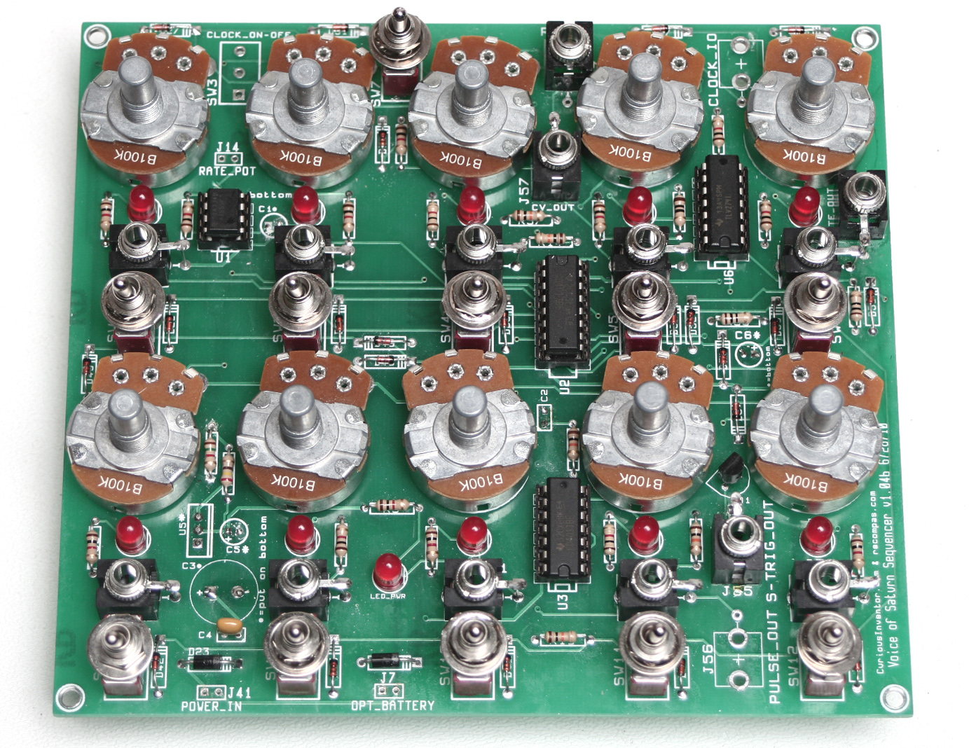
BOM Layout
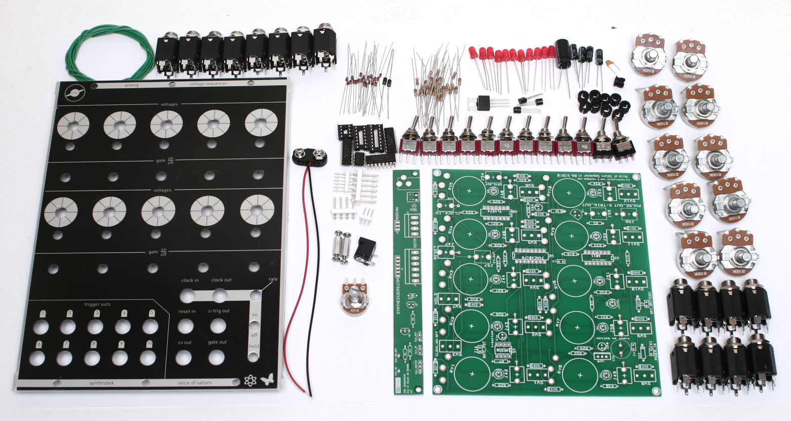
Check your kit against the BOM and verify that all components are present – if anything is missing we will ship it to you free of charge.
Attention: Changes may occur after the assembly instructions are created and the photos may not reflect those changes. Always use the BOM to verify the placement of components.
Resistors, Sockets, Diodes, Transistor and Ceramic Capacitor
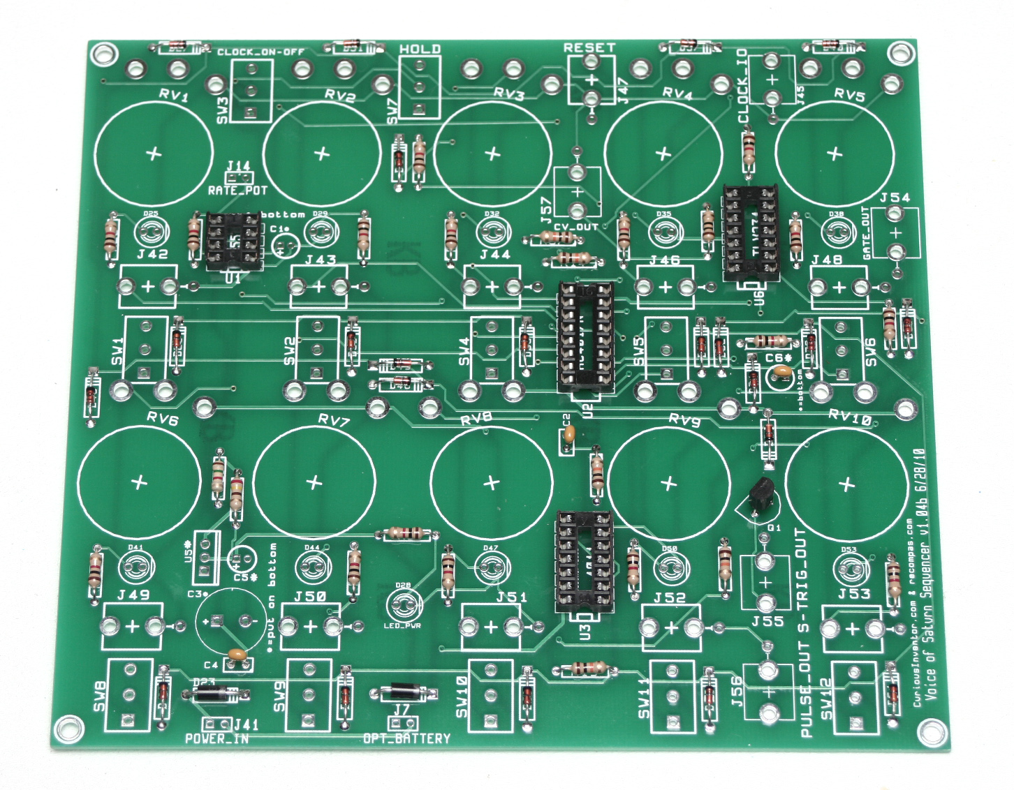 Begin by soldering all resistors, sockets, non-illuminated diodes, and the transistor into place on the primary PCB. Resistors and ceramic capacitors are non-polar components and may be inserted in any orientation. The polarity stripe on each diode must be aligned with the corresponding making on the silkscreen – orient the transistor (Q1) in similar fashion.
Electrolytic Capacitors, Voltage Regulator, 555 Bridge Resistor
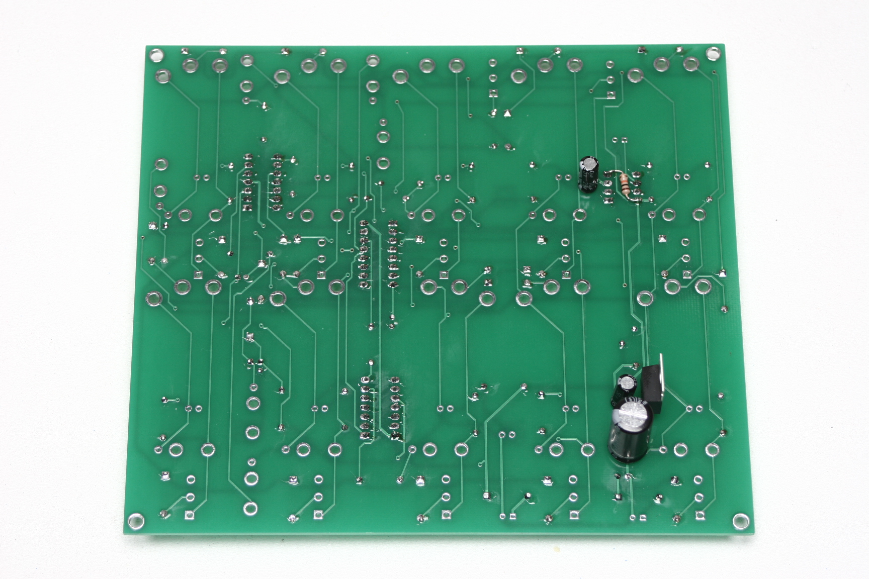
Install the voltage regulator and electrolytic capacitors on the back of the board using the above photo for reference orientation. The polarity markings for the capacitors on the opposite side of the board are correct, but the voltage regulator *must* be oriented opposite the direction indicated by the silkscreen when installed on the back of the board. Solder a 10k resistor between pins 4 and 8 of the 555 timer as shown above.
Using 1/8″ jacks? CLICK HERE. 1/4″ jack users who wish to use their own case or forego an enclosure entirely may disregard further instructions pertaining to front panel mounting and alignment.
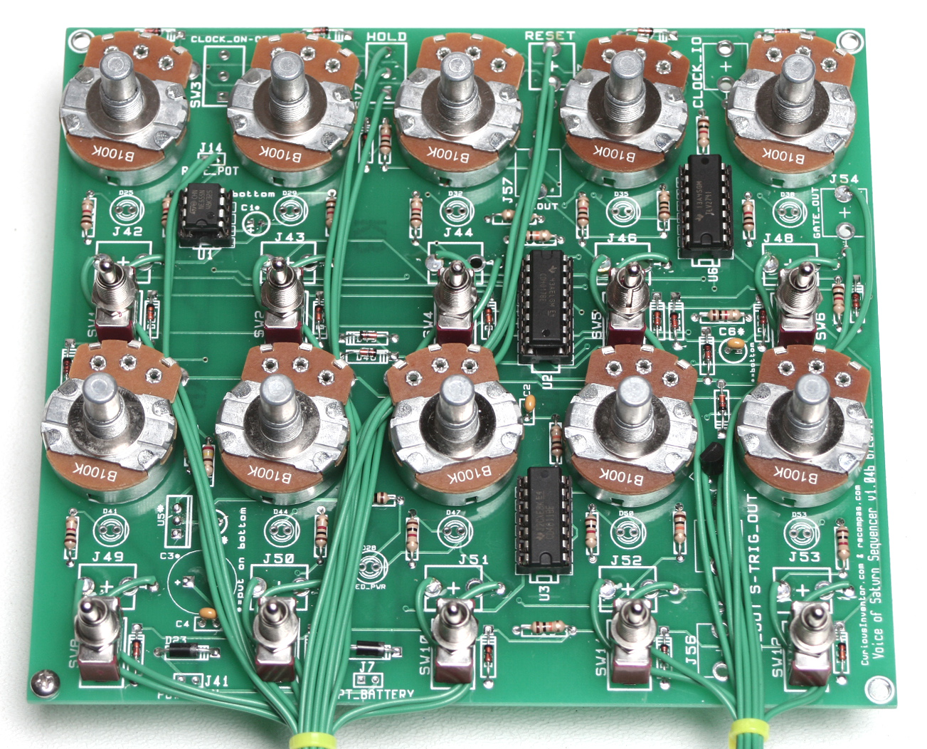
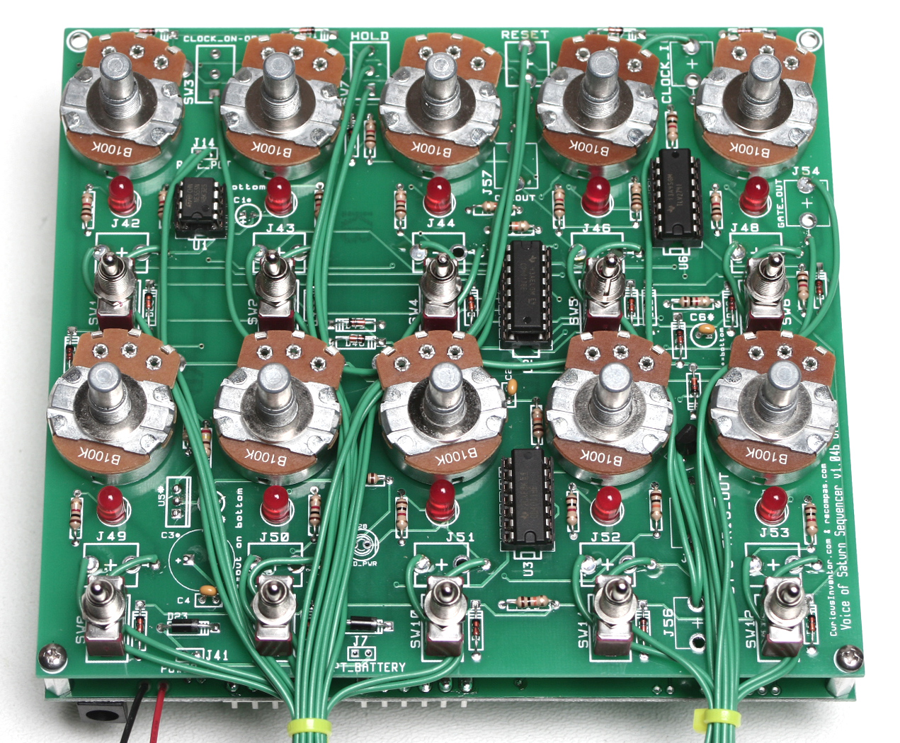
PCB-Mounted Potentiometers & Switches
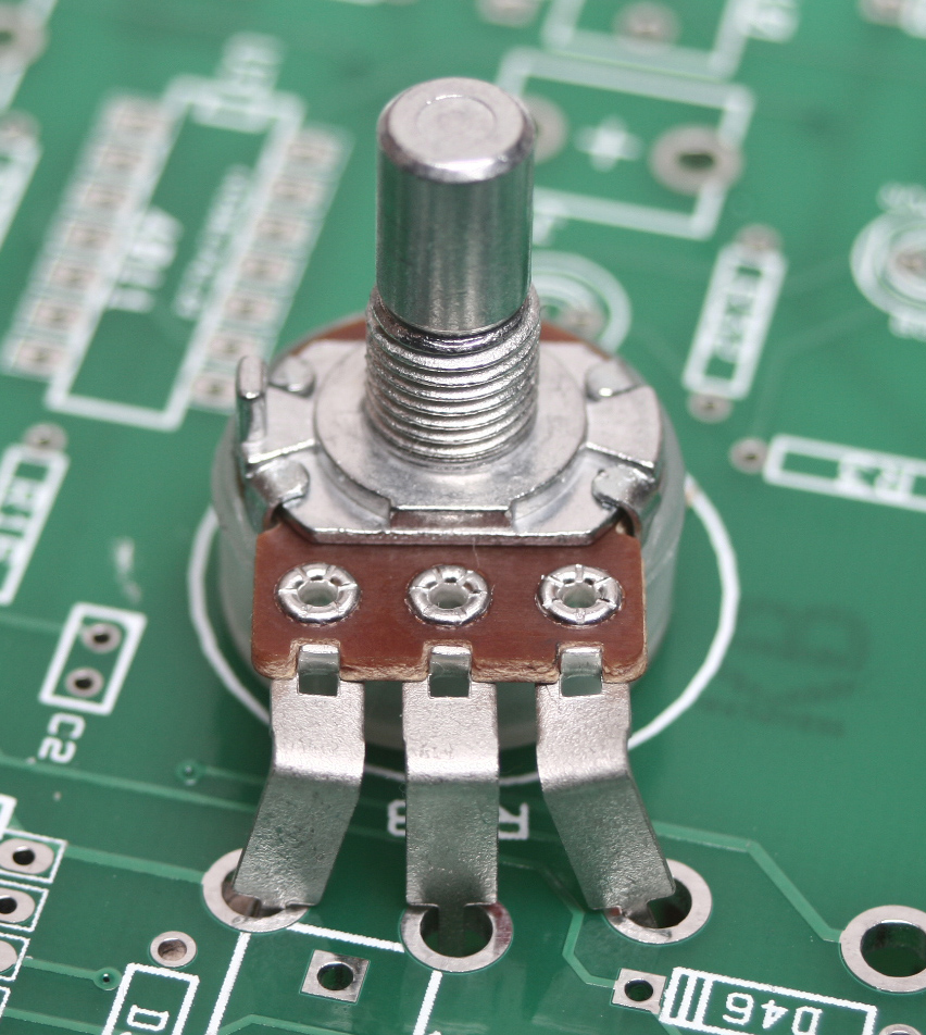
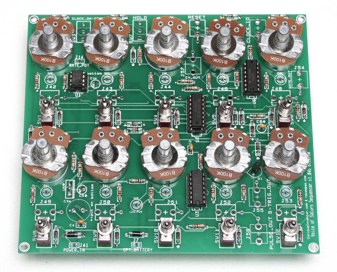 Flip the board over and proceed to insert the ten PCB-mounted 100K linear potentiometers and SPDT switches through the PCB. The SPDT switches have a very snug fit and may require above average force to fully insert. Remove all but one nut from each switch and one washer from each potentiometer to ensure proper spacing, and remove the nubs from the potentiometers prior to inserting them through the PCB:
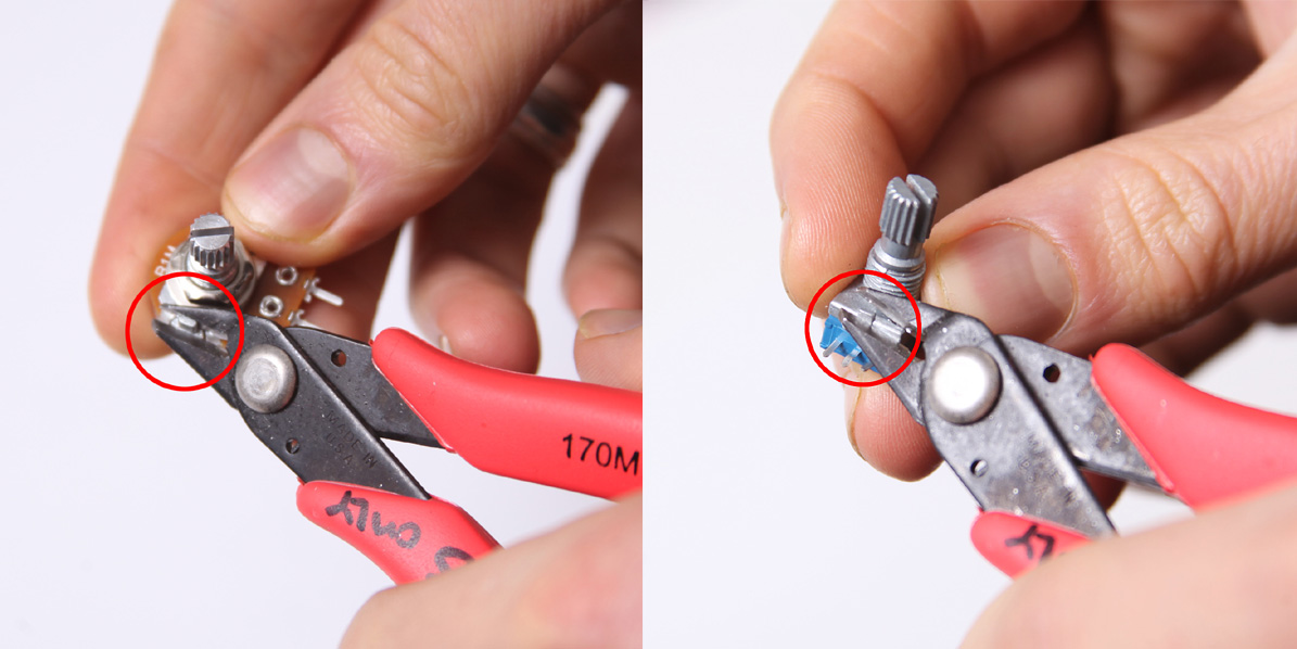
Don’t forget to cut the nubs on the potentiometers as necessary.
Some kits may ship with an alternate style potentiometer not shown in the build photos due to parts availability. Bend the legs for pins 1 & 3 outwards to accommodate the via spacing prior to inserting these smaller potentiometers through the board:
Initial Panel Alignment
Carefully install the panel and verify that it is seated evenly against the SPDT switch. After checking that the panel is seated evenly, use the remaining nuts to secure it in place. It is not necessary to use washers externally as the protective plastic will prevent the panel from scratching. Excessive force may cause the plastic to tear however, and it is advisable to use minimum amount of torque.
Flip the sequencer over and solder the potentiometers and switches in place – clip the potentiometer leads afterwards.
Preliminary Panel Wiring
Remove the faceplate and solder leads for all wired components using the photo above for reference. It is not necessary to connect the ring shunt contact on any of the jacks except J47 – the reset jack utilizes the ring shunt in place of the sleeve contact. Do not run wires from J56 (PULSE_OUT), J45 (CLOCK_IO), or SW3 (CLOCK_ON_OFF). It is advisable to use slightly more wire than necessary to reach each component and label the end of each lead, as all wired components are installed once the front panel is mounted in place. It is not necessary to route the front panel wiring through the legs of the pots and switches, but doing may provide helpful strain relief when reinstalling the front panel. Zip ties (shown above) may prove useful for additional wire management.
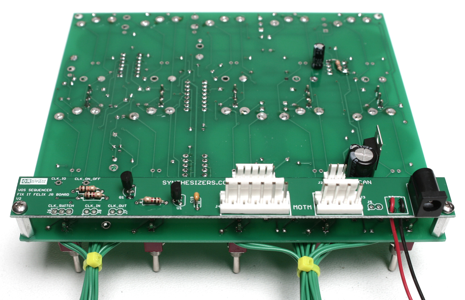
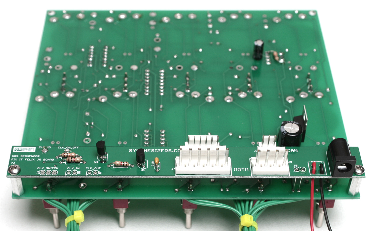
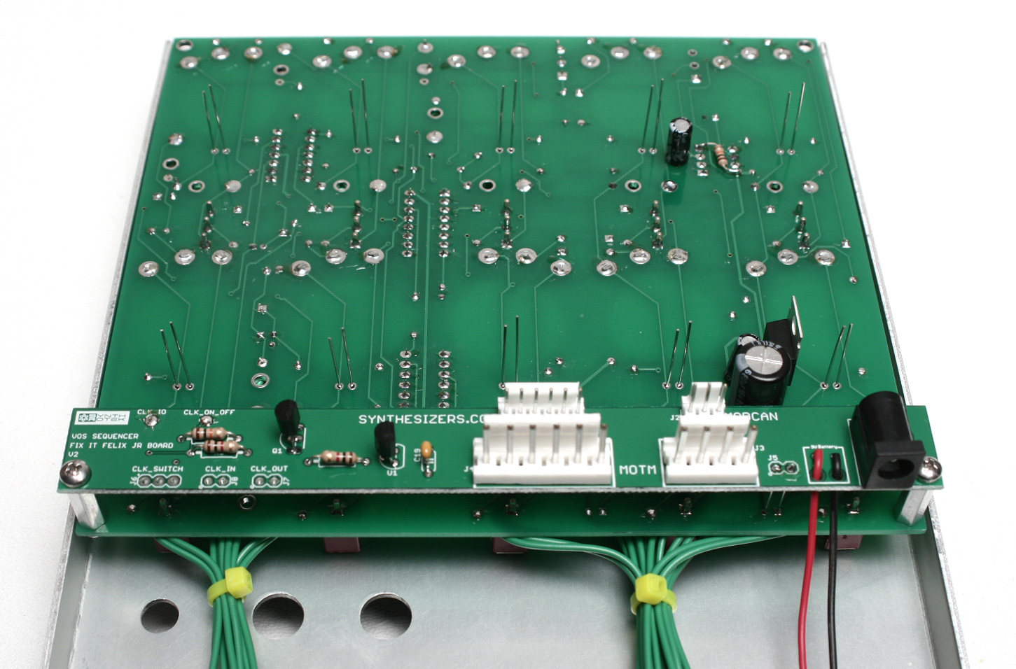
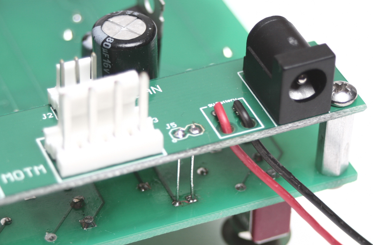
Mod Board Assembly & Installation
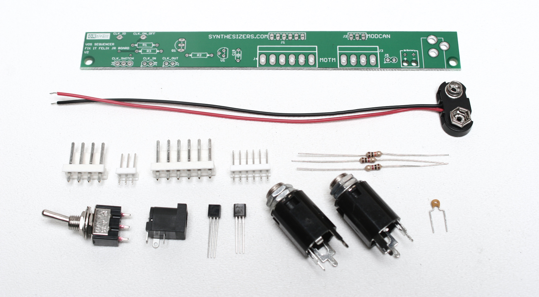
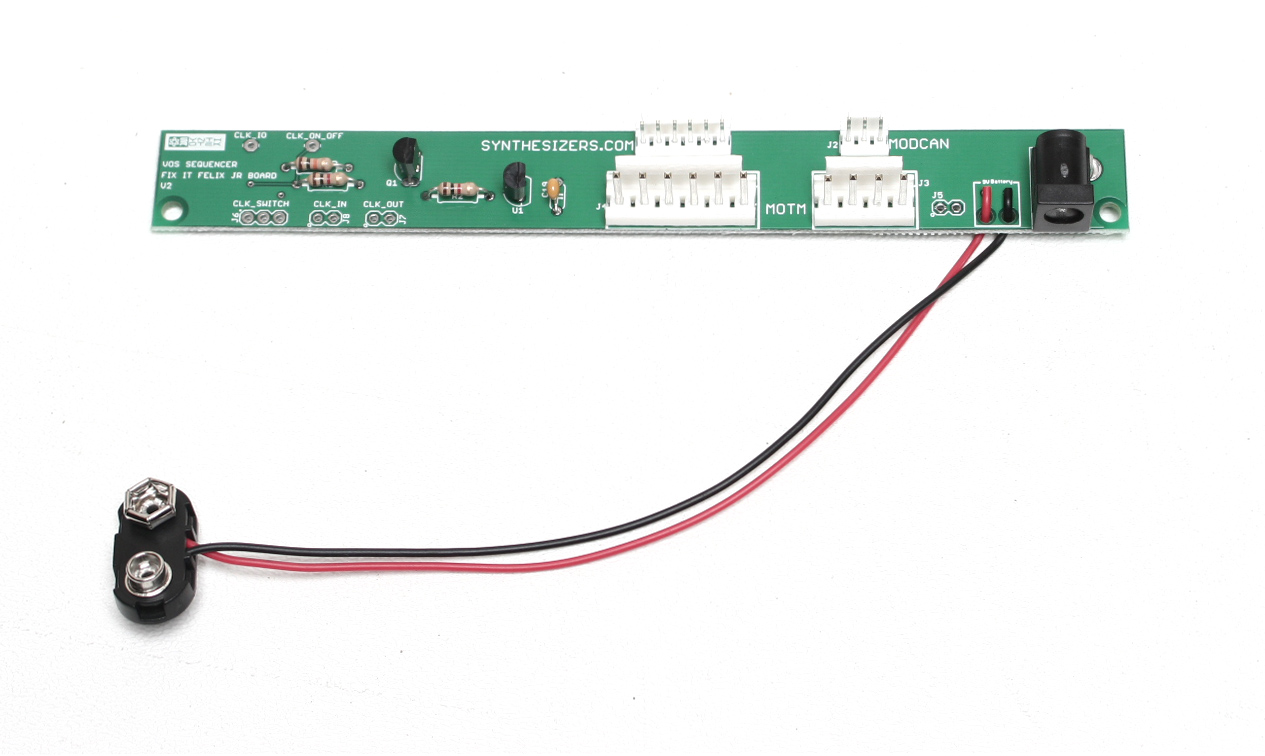
All components required to assemble the mod board are shown above – kits will only come with the power connector option(s) specified at checkout. Solder all components to the mod board with the exception of the clock in/out jacks and clock on/off switch:
Attach the included metal standoffs to the primary board using the supplied phillips screws:
Attach the mod board to the standoffs using the remaining two phillips screws:
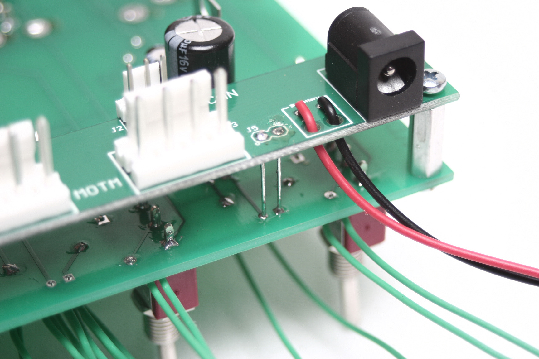
Use two resistor/capacitor legs to connect J5 on the primary board to J41 on the mod board using the photo below for reference:
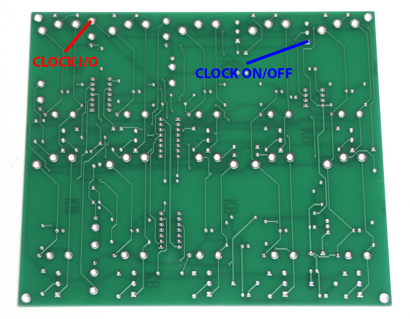
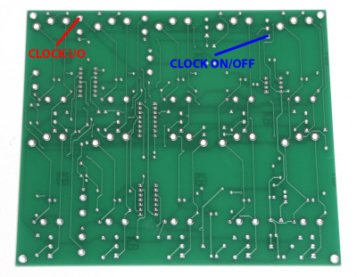
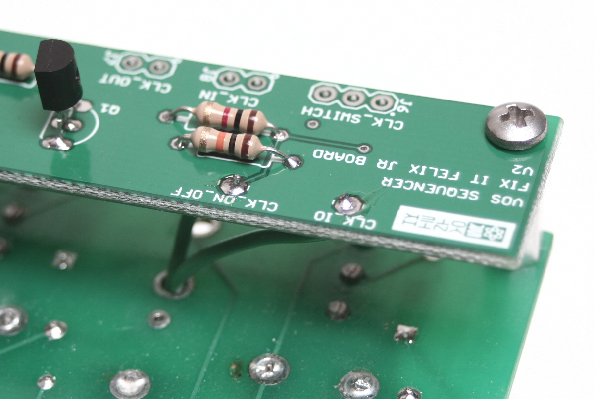
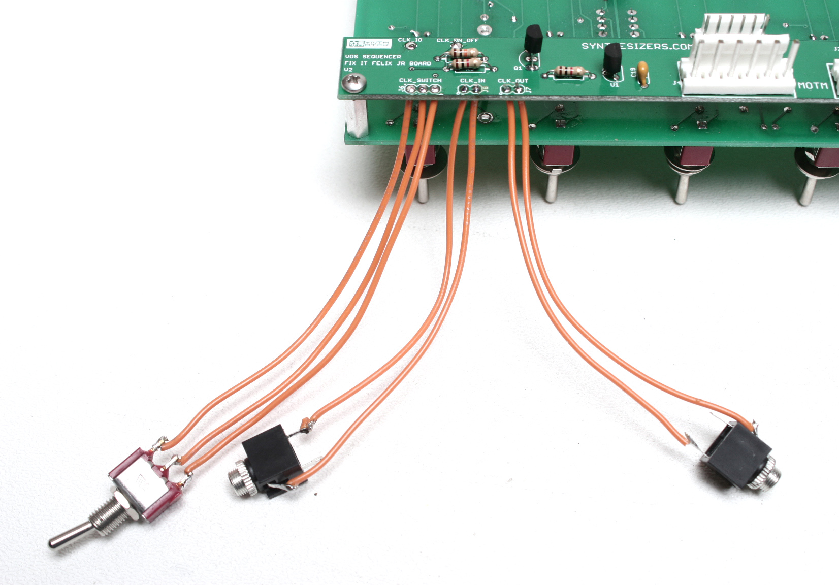
Solder relatively short wired leads to J6 (CLK_SWITCH), J7 (CLK_OUT), and J8 (CLK_IN) on the mod board – 2-3″ will suffice. Connect longer wired leads from CLK_IO and CLK_ON-OFF to the following points on the PCB:
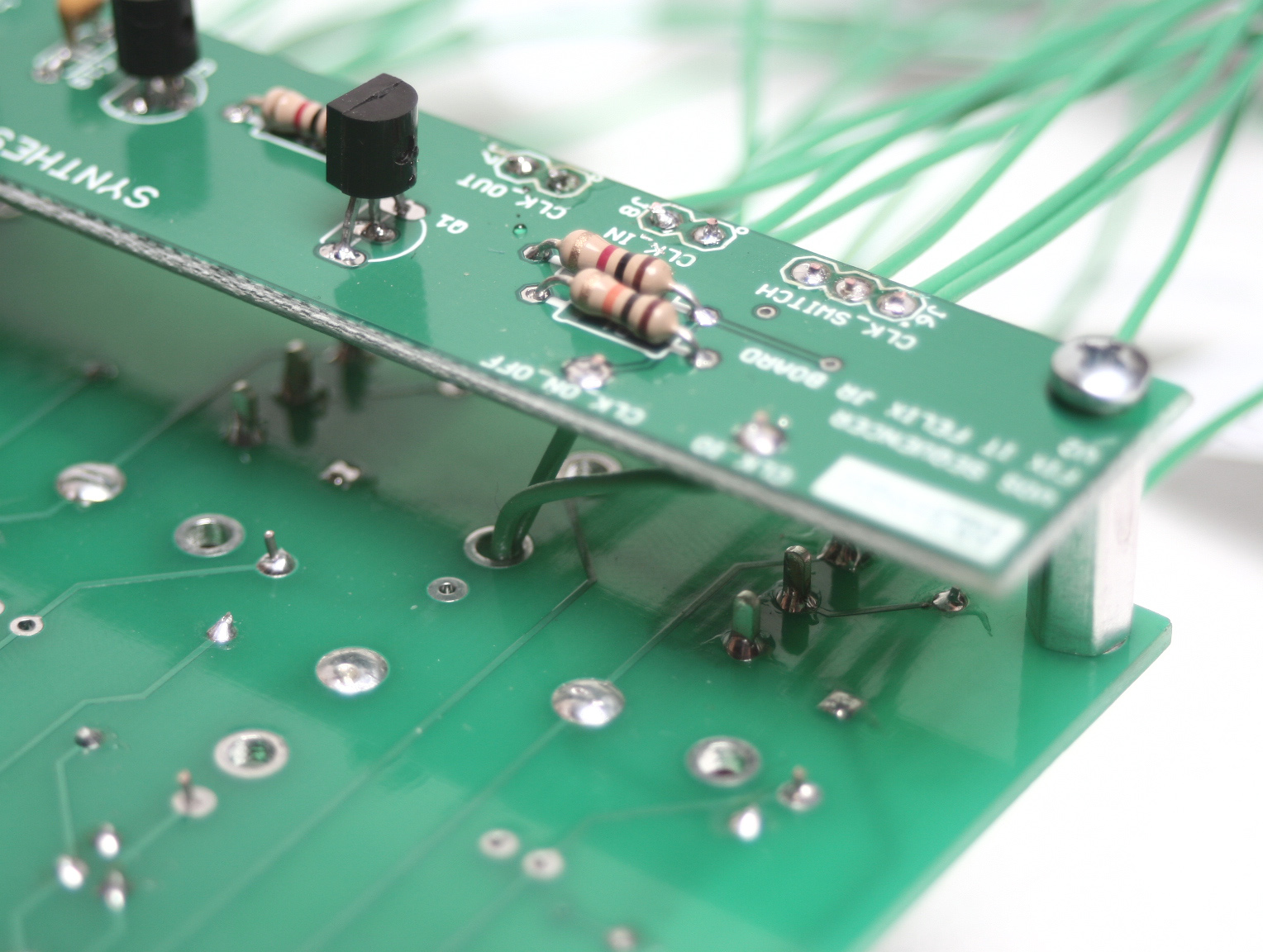
You may choose to route the wiring for these connections through the unused PULSE_OUT vias (J56) and across the front of the board – doing so will keep exposed wiring to a minimum. See the photo below for reference:
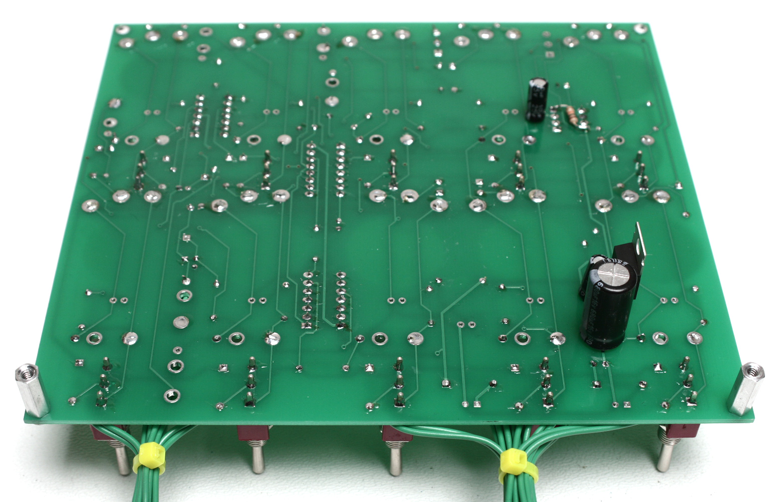
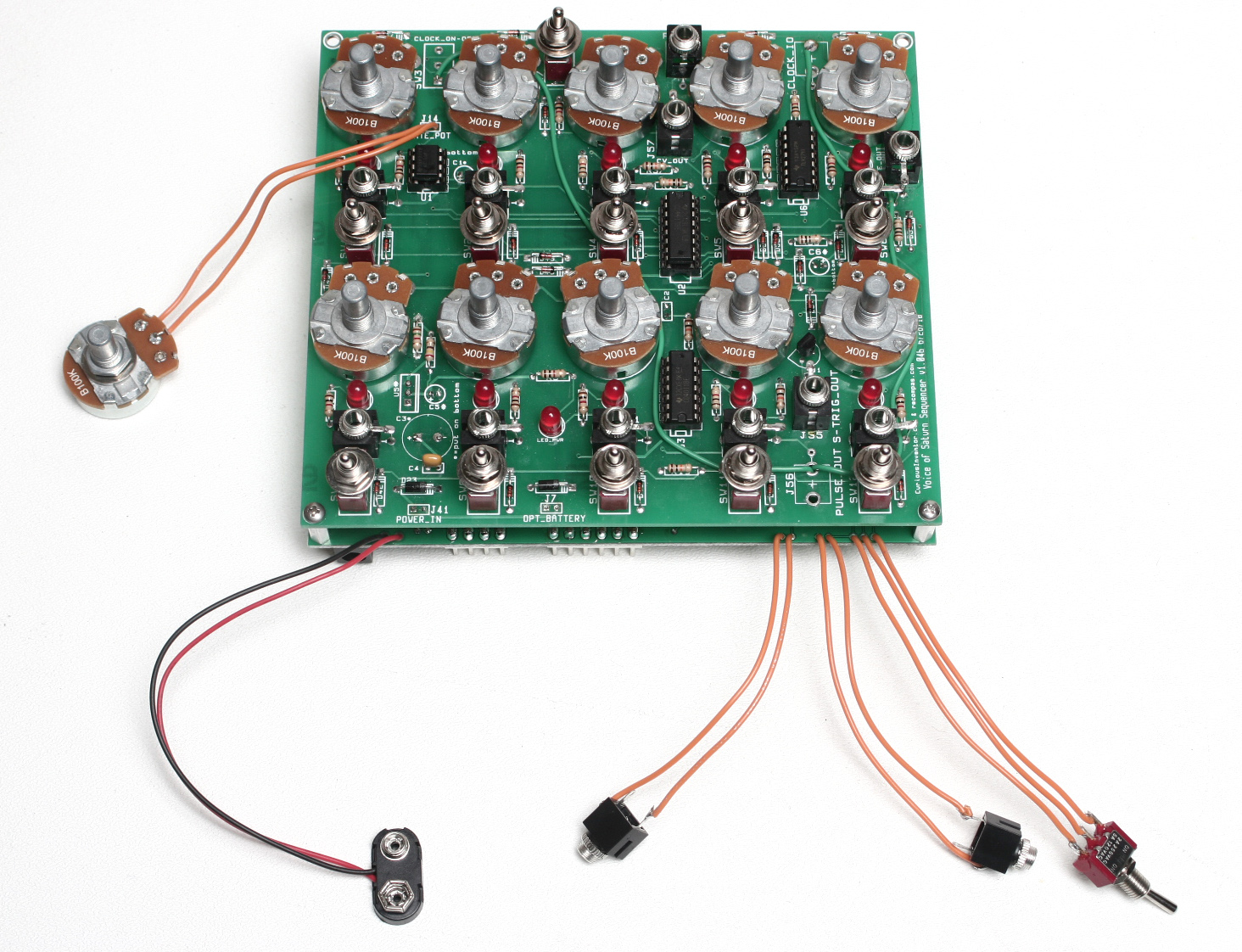
Now that the mod board is in place, ensure all wire leads are tidy and routed parallel to the vertical edge of the primary board:
LEDs & Faceplate
Now you are ready to finalize the front panel! Flip the sequencer over and insert an LED below each potentiometer – be sure to align the flat side of the LEDs with the corresponding markings on the silkscreen:
Remove the protective plastic from the faceplate and insert the ten plastic LED mount grommets through the corresponding holes. Reinstall the front panel, ensure it is seated evenly against the pots/switches, and secure in place with the relevant nuts. Externally visible washers are optional and may be discarded if not used. Flip the sequencer and insert the the LEDs through the grommets:
Ensure the the LEDs are seated evenly prior to soldering in place. It is not possible to fully insert the LEDs through the grommets due to a lack of physical access, but they can be inserted to a depth sufficient for visibility.
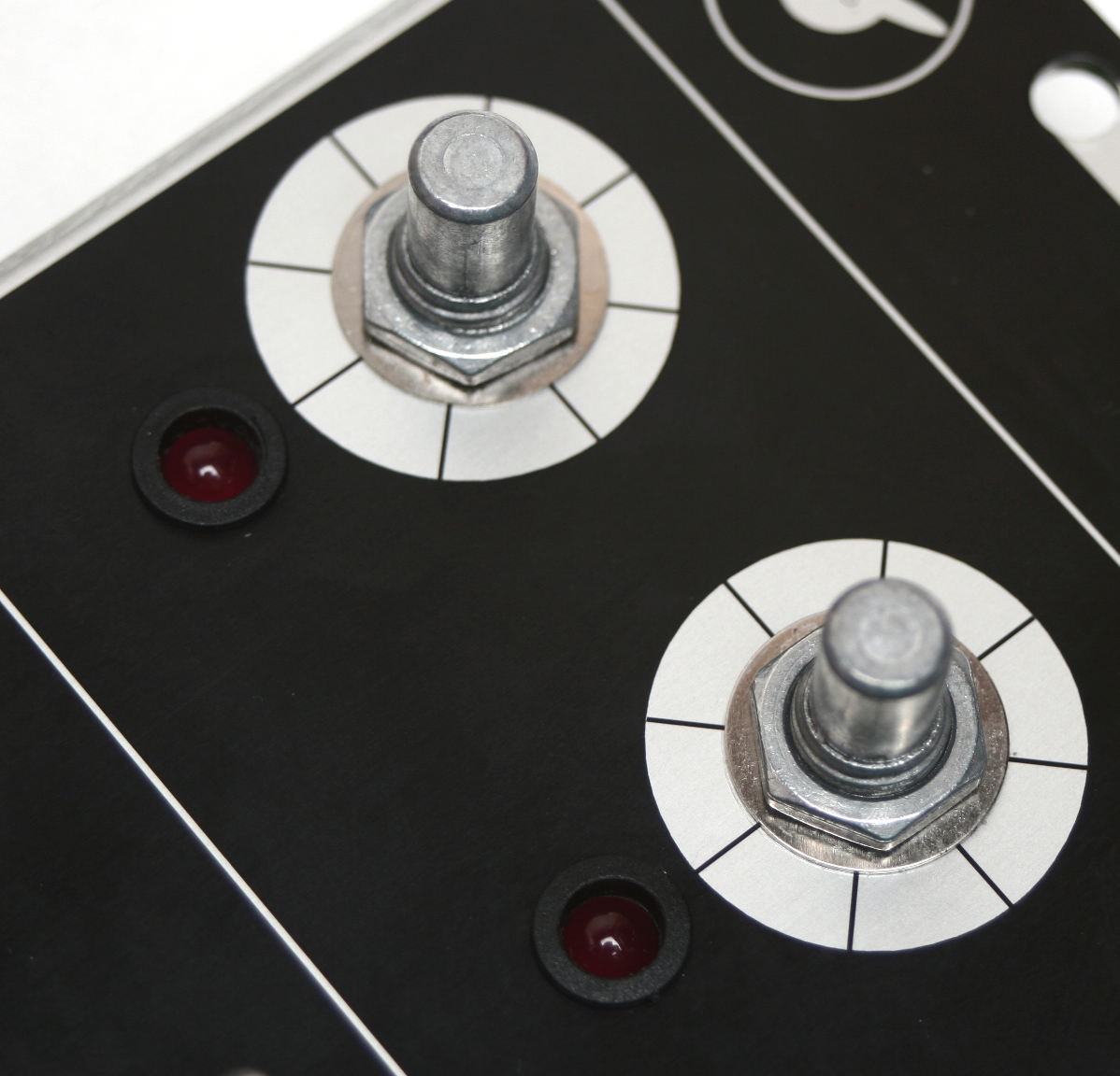
The above photo demonstrates the approximate maximum insertion depth achievable with the panel mounted in place. Once the LEDs are inserted through the grommets and aligned at similar depths, solder them in place and trim the excess lead length.
Wired Components
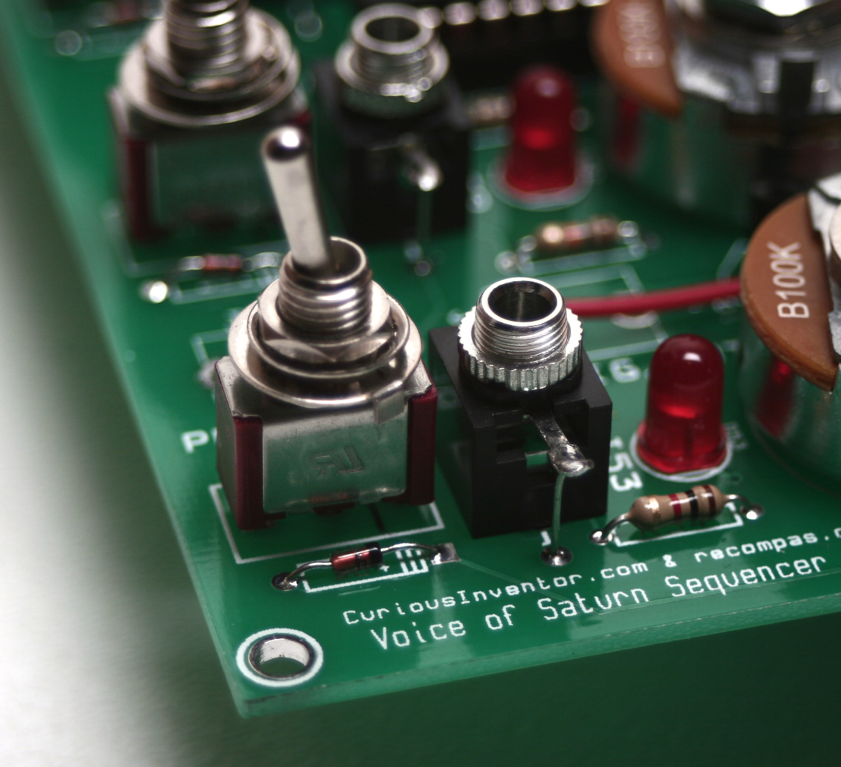
Mount the remaining quarter inch jacks and SPDT switches to the lower section of the front panel. Washers are not used on the two SPDT switches or rate potentiometer and are optional for the 1/4″ jacks. Match each set of leads with the corresponding jack/switch, trim the leads to the appropriate length, and solder in place. If you opted to forego individually labeling each wire, a multimeter may be used to determine lead continuity from the backside of the board.
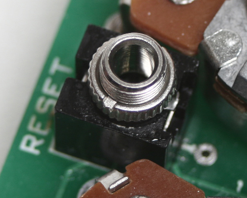
All 1/4″ mono jacks should be wired using the tip and sleeve contacts with the exception of the reset jack, which utilizes the ring contact instead of sleeve. The photo below provides a detailed look at the wiring connected to the reset jack and mod board:
Note that the circular silkscreen markings on J7 (CLK_IN) and J8 (CLK_OUT) indicate polarity of the adjacent contact (tip).
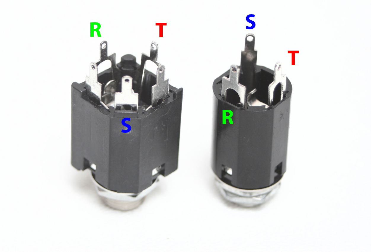
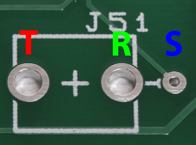
The above photos provide a pinout of both jack styles in addition to corresponding contacts on the PCB.
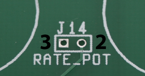
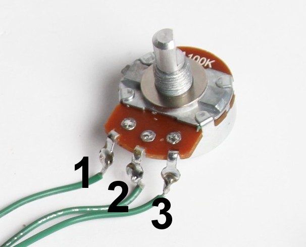
The square and circular vias of J14 (RATE_POT) must be connected to pins three and two on the B100K potentiometer, respectively. See the photos below for reference:
Once the front panel wiring is finished, your sequencer is complete and ready for testing!
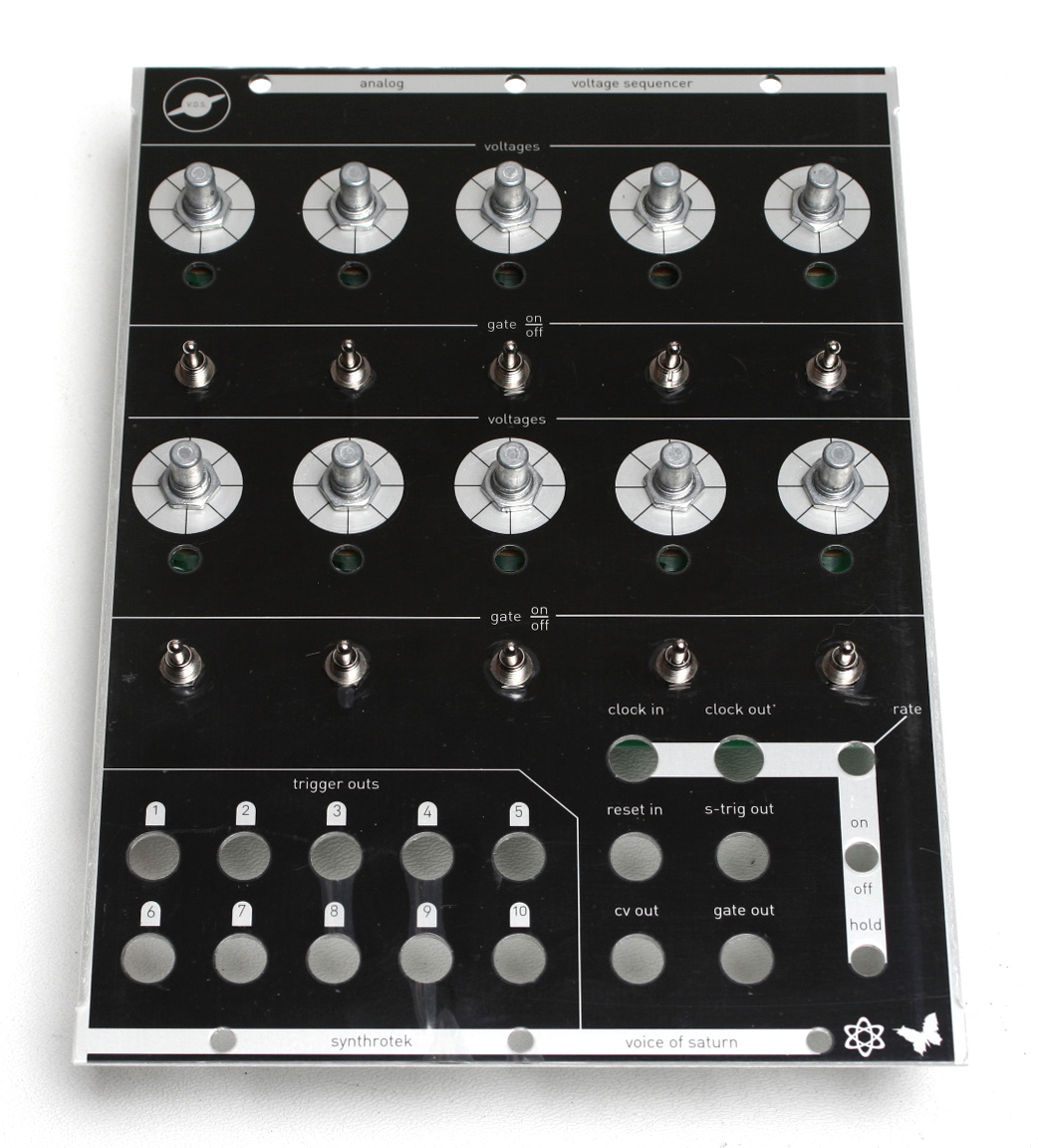
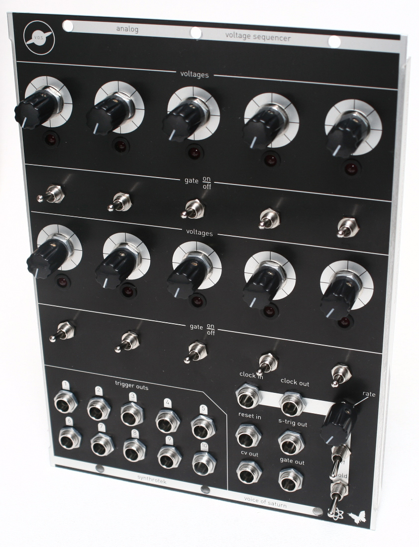
Completed Project
1/8″ Jack Assembly – PCB Mounted Components
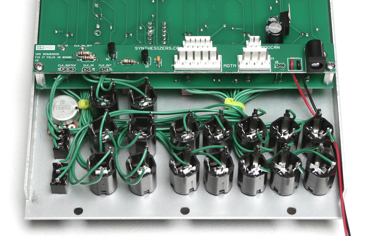
 Although it is not necessary to mount components directly to the PCB, utilizing 1/8″ jacks enables board-mounting nearly all potentiometers, jacks, and switches – the notable exceptions being the rate potentiometer, clock on/off switch, and clock I/O jacks. Flip the board over and insert the ten B100K potentiometers, eleven SPDT switches, eleven LEDs, and fourteen 1/8″ jacks using the photo above for reference. Ensure all components are flush with the board, solder them in place, and trim excess lead length from the back of the board. Do not populate SW3 (CLOCK_ON_OFF), J45 (CLOCK_IO), and J56 (PULSE_OUT, unused). The SPDT switches have a very snug fit and require above average force to fully insert. Use a resistor/capacitor leg to connect the sleeve contact to the PCB on each 1/8″ jack barring reset:
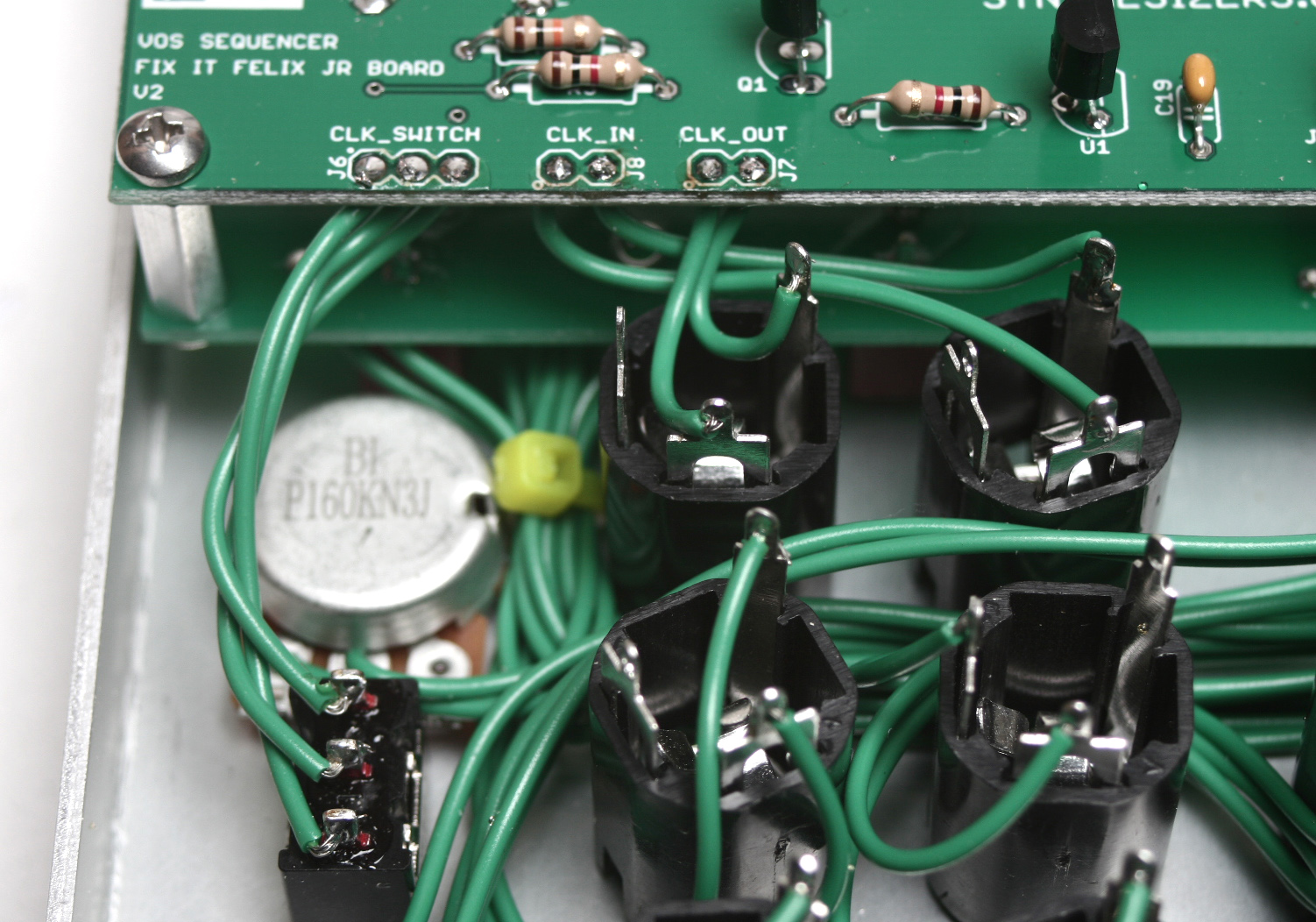
The sleeve contact on the reset jack should not be connected and may be removed entirely:
Some kits may ship with an alternate style potentiometer not shown in the build photos due to parts availability. Bend the legs for pins 1 & 3 outwards to accommodate the via spacing prior to inserting these smaller potentiometers through the board:
Mod Board Assembly & Installation
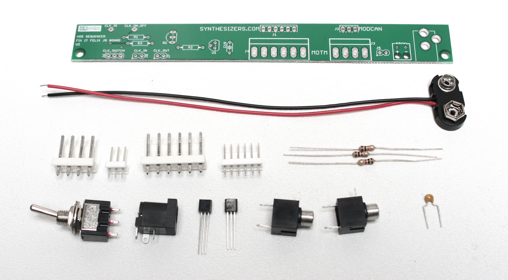
All components required to assemble the mod board are shown above – kits will only come with the power connector option(s) specified at checkout. Solder all components to the mod board with the exception of the clock in/out jacks and clock on/off switch:
Attach the included metal standoffs to the primary board using the supplied phillips screws:
Attach the mod board to the standoffs using the remaining two phillips screws: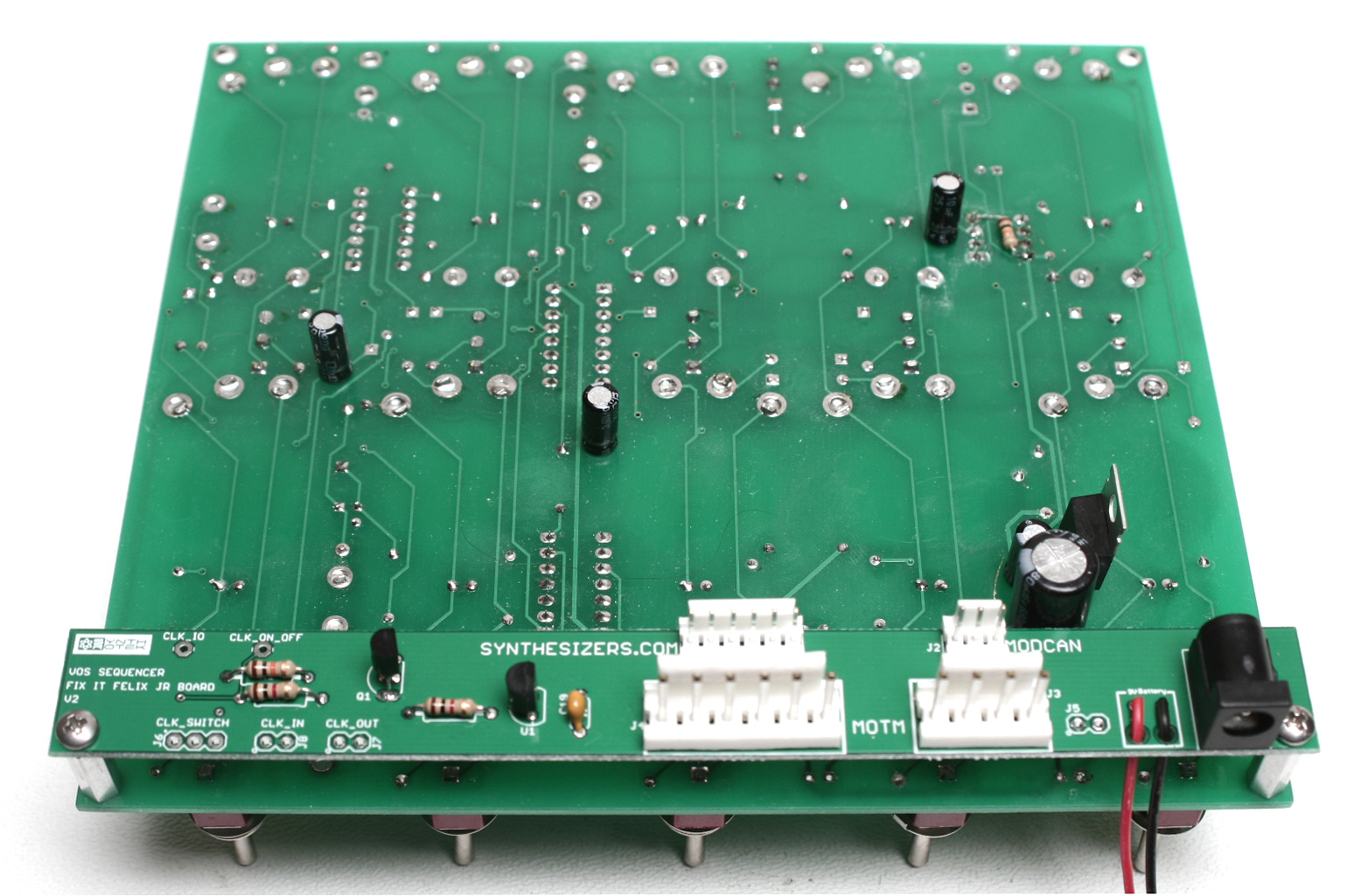
Use two resistor/capacitor legs to connect J5 on the primary board to J41 on the mod board using the photo below for reference:
Connect longer wired leads from CLK_IO and CLK_ON-OFF to the following points on the PCB:
You may choose to route the wiring for these connections through the unused PULSE_OUT vias (J56) and across the front of the board – doing so will keep exposed wiring to a minimum. See the photo below for reference:
Wired Components
Solder wired leads of the desired length to the remaining SPDT switch and eighth inch jacks. Connect to the mod board using the below photo for reference:
Note that the circular silkscreen markings on J7 (CLK_IN) and J8 (CLK_OUT) indicate polarity of the adjacent contact (tip). The sole remaining wired component is the rate potentiometer. The square and circular vias of J14 (RATE_POT) must be connected to pins three and two on the B100K potentiometer, respectively. See the photos below for reference:
Your sequencer is complete and ready for testing once wired components are installed!
can i get the silk screened front panel separate?
Vince
We’re not selling them separately at this time, sorry Vince.
DIYed this piece and it worked great. Began plugging things in here and there and now it wont advance to the next step without me throwing the hold switch. Flipping Clock on/off does nothing to fix this. Have you encountered anything like this and if so, did you find a solution?
Craig,
I haven’t encountered this yet. The first thing would be to unplug everything and then see if you can get it to start going again. I would also double check that your switches are working properly, and that there isn’t a break in the wire between any of the switches and the board. For further support, you can email us at store@synthrotek.com
Best,
-Patrick
c6 has a +sign on it, also i’m missing a couple components who do i speak with to get them replaced?
So is c6 an electrolytic or ceramic capacitor??
Damn! Just finished this. Doesn’t work. Won’t even light up. Followed the pics above and it seemed pretty easy/straightforward. Such a bummer.