


PT2399 DIY Delay PC BOARD ONLY
May 10, 2010New Project Boards are FINALLY here!!!
July 22, 2010This product has been discontinued, but we replaced it with a better one! Check out the PT2399 Dev Delay.
Welcome to the PT2399 Lo-Fi Assembly Instructions Guide! Let’s get started building our circuit!
BOM (Bill of Materials)

The best way to start any electronics project is to lay out your parts and identify them. If this is your first electronics project, don’t worry – we will identify each part in this section to have familiarize you with them.
Ceramic Capacitors

The ceramic capacitors have codes for the capacitance values written on them. If you are having trouble identifying each of these capacitors, take a look at the following cheat sheet:

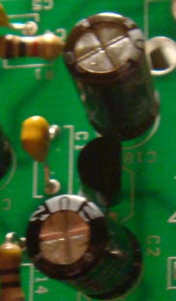
Electrolytic Capacitors

Electrolytic capacitors are polarized, which means we will have to pay special attention when placing them on our PCB.
LED (Light Emitting Diode)

The LED will be used to indicate our circuit is on and that it is connected to the power supply. Notice that one lead is longer than the other. The shorter lead indicates negative polarity and the longer lead indicates positive polarity.
Schottky Diode

Schottky diodes act as valves, allowing current to flow in one direction only. They are used in the circuit to prevent damaging the circuit by plugging in a power source incorrectly. If you look closely, you will see a black band near one lead. This designates the lead as negative.
Resistors and Potentiometers

Resistors dissipate current as heat. They are used to regulate voltage flow. The value of a resistor is determined by its color code. 4 bands of color are on each resistor, but we only need to pay attention to the first 3 (the 4th, gold, is common to each and indicates the resistor’s tolerance). If you are new to electronics, this cheat sheet will help you:

1/8″ Mono Audio Jacks

These jacks are used for input and output signals. They have three connections, two of which we will use in our circuit.
A/C Adapter Jack

This component allows us to use A/C adapters (“wall warts”) with our circuit.
9V Battery Connector

Found in many musical electronics, the 9V battery connector connects to a 9V battery.
PCB (Printed Circuit Board)

A PCB is extremely useful for speedy circuit building. The top layer is where our components will be inserted.

The bottom layer of our PCB is where we will be soldering our leads and wires.
Voltage Regulator

This component ensures our circuit will be provided with a constant voltage level. Its body has a rounded side and a flat side, which will be important during assembly for orienting the component.
PT2399 IC (Integrated Circuit)

The PT2399 is the heart of our circuit, providing it with the Delay functionality. Note the small dot next to the half-circle notch on the left side – this indicates that Pin 1 is at the bottom-leftmost position.
* Note – Many ICs (like the PT2399) are sensitive to static electricity. If your workspace is on a rug and/or you live in a dry environment, it is very likely that you are conducting electricity through your body. This tiny amount of voltage can damage sensitive components and . So take the following precautions:
– Leave all ESD(Electrostatic Discharge)-sensitive components in their packages until they are ready to be used
– Ground yourself before touching any ESD-sensitive components by touching something metallic or using an anti-static wrist strap.
Assembly
1. IC

In the picture above, we see the outline of U1, our PT2399 IC. Notice how there is a square overlay at the lower left hand position. This is where Pin 1 of the IC will be placed and off of which the rest of the pins will be aligned. If the pins on the IC are too wide to fit into the holes, gently squeeze them inward after discharging any static electricity your body may have accumulated.

Once the IC is in place, flip the board over and solder the leads.
2. Ceramic Capacitors

Locate the positions for the ceramic capacitors and insert each into its respective through-holes. Bending the leads in opposite direction on the back to the PCB helps retain their position. Solder and clip the excess wire.
3. Resistors

Place the resistors in their positions, solder, and clip the excess lead wire.
4. Electrolytic Capacitors

Electrolytic capacitors are polarized, meaning that they have a positive lead and a negative lead. Improper positioning can damage your circuit, so it is good to double-check how they are inserted before soldering. On the PCB, the negative leads are identified by a square overlay around the through-hole.

Once the electrolytic capacitors are positioned, solder them to the PCB and cut the excess lead wire.
5. Schottky Diodes

The two diodes will be placed onto the PCB like any other polarized component – the negative lead goes into the square overlay through-hole and the positive lead goes into the circle overlay through-hole.

Because of their small size, you may need a magnifying glass to see the negative-lead-identifying black band.
6.Voltage Regulator

To insert the voltage regulator, look at the silkscreen overlay on the top of the PCB. The outline makes the placement obvious enough. The leads may need to bent outward to fit into all of the through-holes. Bend the leads to retain the position and solder the voltage regulator to the PCB. Clip the excess lead wire.
7. 1/8″ Mono Audio Jacks

Solder two wires to each jack as shown in the picture above.

J2 and J3 are where our wires are going to be inserted and soldered to.

Using colored wire helps to identify which wire goes to what position. Solder the wires and clip the excess wire.
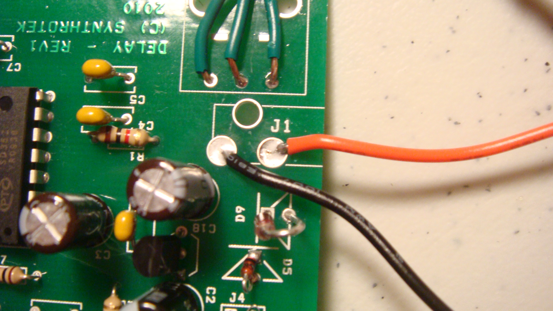
8. A/C Adapter Jack

Solder two wires onto the solder terminals of the A/C adapter jack as shown in the picture above.

Using the wires we just soldered to our A/C adapter jack, insert into J1. One through-hole is not used. Using solder on the rims of the through-holes before inserting the wires helps to keep the soldering tidy.
9. Potentiometers

Connect three wires of equal length to each solder terminal of the potentiometers. Using a lot of bare wire can help make a strong physical connection, which makes for a strong and solid solder connection.
")

Connect the potentiometer wire using the colored circles as a reference.
10. 9V Battery Adapter

Insert the black wire into the square overlay through-hole and the red wire into the circle overlay through-hole. Make sure to make a strong solder joint, as 9V battery connection wires are notoriously brittle.
11. LED

Insert two wires in D1’s through-holes as shown in the picture. The black wire will go to the shorter lead of the LED and the red wire will go to the longer lead.

At this point, you have a choice to make: if you are going to case-mount your circuit, hold off on soldering the wires to the LED right now. This type of LED is meant for mounting and has a wider top than the rest of the body. By soldering to it now, you may have to de-solder the LED when you are ready to mount your circuit.
Congratulations, you have finished constructing your PT2399 Lo-Fi Delay circuit! The next part of this guide deals with mounting this circuit. Following the case mount guide, you can learn how you can modify your circuit for stompbox functionality and to utilize 1/4″ jacks.
Case Mounting
Coming soon…
Modifications
Coming soon…
Adding 1/4″ Jacks
Coming soon…
Adding a Stompbox Bypass Switch
Coming soon…
SPST Switch with DPDT Relay
Coming soon…
DPDT Switch
Coming soon…